
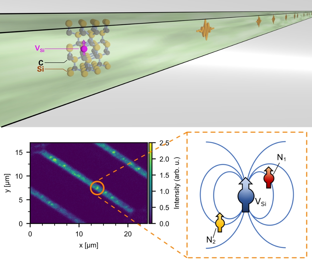
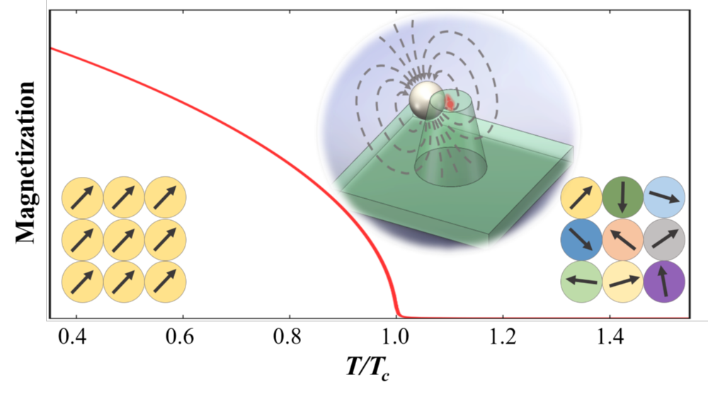
The integration of colour centres into nanophotonic structures enables a high photonic efficiciency, one of the key requirements for quantum technologies. However, nanostructuring and the involved fabrication processes can decrease the spectral stability of integrated colour centres. In our recent work, we systematically investigate these parasitic effects on silicon vacancy colour centres in 4H-silicon carbide by fabricating membranes with thicknesses in the range of 3 µm to 0.25 µm starting from bulk material with integrated silicon vacancies.
Our first key result shows that the spectral position of the zero-phonon-line (ZPL) emission spreads more with a decreasing membrane thickness and bulk ZPL positions can be partially recovered by a post-fabrication annealing. For the second key result, we study V2 center properties under photoluminescence-excitation (PLE) measurements. As expected, we find that the PLE linewidths and spectral jumping increases with a decrease of the membrane thickness. We conclude a membrane thickness of ~ 0.6 µm seems to be a good sweet spot where most of the emitters show bulk-like PLE properties.
Reference:
Heiler, J., Körber, J., Hesselmeier, E. et al. Spectral stability of V2 centres in sub-micron 4H-SiC membranes. npj Quantum Mater. 9, 34 (2024).

Quantum state readout is a key requirement for a successful qubit platform, because it enables precise measurements and active-feedback algorithms.
In this work, we demonstrate a high-fidelity quantum state readout of a V2 center nuclear spin based on a repetitive readout technique by exploiting the long spin lifetime of a strongly coupled nuclear spin.
We demonstrate up to 99.5% readout fidelity and 99% for state preparation. Using this effective readout, we initialize a nuclear spin by measurement and demonstrate its Rabi and Ramsey nutation, which even shows coupling to a second nuclear spin. Finally, we use the nuclear spin as a long-lived memory for quantum sensing application of weakly coupled nuclear spins, revealing a diatomic spin bath.
References:
High-Fidelity Optical Readout of a Nuclear-Spin Qubit in Silicon Carbide, Erik Hesselmeier, Pierre Kuna, et al. Phys. Rev. Lett. 132, 180804
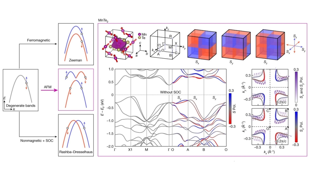
The research field of spintronics based on antiferromagnetic (AFM) materials paths the way for a new generation of spintronic devices, which, for example, can generate and manipulate spin-polarized currents.
Recently, theory predicted a new type of spin splitting in selected antiferromagnets. This splitting cannot be explained by Zeeman or Rashba-Dresselhaus interaction. Instead, it is induced by long-range magnetic order even when spin-orbit coupling is absent and leads to a giant and momentum-dependent spin polarization of energy bands in the antiferromagnet. However, a spectroscopic evidence of such spin splitting is still missing.
In this study, our collaborators demonstrate the existence of this AFM-induced spin splitting in the noncoplanar antiferromagnet MnTe2, utilizing spin-resolved and angle-resolved photoemission spectroscopy (SARPES) measurements and theoretical analysis. They uncover a quadratic spin-splitting effect with a plaid pattern in the spin texture. This effect is induced by magnetic exchange and is therefore distinct from the Zeeman or Rashba-Dresselhaus scenarios.
Our contribution to this work is the investigation of the AFM domain structure of MnTe2 with our new low temperature scanning probe magnetometer based on the nitrogen vacancy center in diamond. We confirm the AFM nature of the material and show over a larger scan area of 50 µm the absents of AFM domain walls. This result supports the argumentation of our collaborators, as it confirms that the AFM domains are larger than the incident beam used for the SARPES measurements.
References:
Observation of plaid-like spin splitting in a noncoplanar antiferromagnet; Yu-Peng Zhu, Xiaobing Chen, Xiang-Rui Liu, Yuntian Liu, Pengfei Liu, Heming Zha, Gexing Qu, Caiyun Hong, Jiayu Li, Zhicheng Jiang, Xiao-Ming Ma, Yu-Jie Hao, Ming-Yuan Zhu, Wenjing Liu, Meng Zeng, Sreehari Jayaram, Malik Lenger, Jianyang Ding, Shu Mo, Kiyohisa Tanaka, Masashi Arita, Zhengtai Liu, Mao Ye, Dawei Shen, Jörg Wrachtrup, Yaobo Huang, Rui-Hua He, Shan Qiao, Qihang Liu & Chang Liu; Nature volume 626, pages 523–528 (2024)
Three-dimensional semiconductor chip architectures promise high-density memories and vastly increased computational speeds. Currently, however, self-heating and leakage currents severely limit the overall performance.
Revealing these issues in situ through current density mapping is crucial, yet non-destructive imaging techniques have been limited to the two-dimensional analysis only.
In this study, we use ensembles of nitrogen-vacancy centers in diamond as nanoscale quantum sensors to probe all three vectorial components of magnetic fields associated with electric currents. We apply this technique to non-invasive imaging of three-dimensional currents in modern multi-layer integrated circuits. We also demonstrate a reliable detection of operational and non-operational chips.
Besides this technical application, further improvements of our technique can provide new insight into the local conductance of materials in condensed matter physics.
References:
Marwa Garsi, Rainer Stöhr, Andrej Denisenko, Farida Shagieva, Nils Trautmann, Ulrich Vogl, Badou Sene, Florian Kaiser, Andrea Zappe, Rolf Reuter, and Jörg Wrachtrup; Phys. Rev. Applied 21, 014055
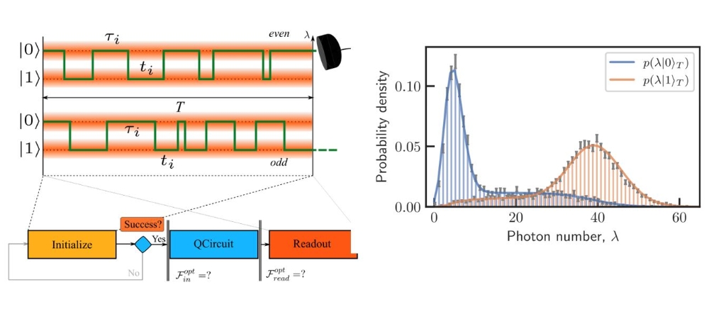
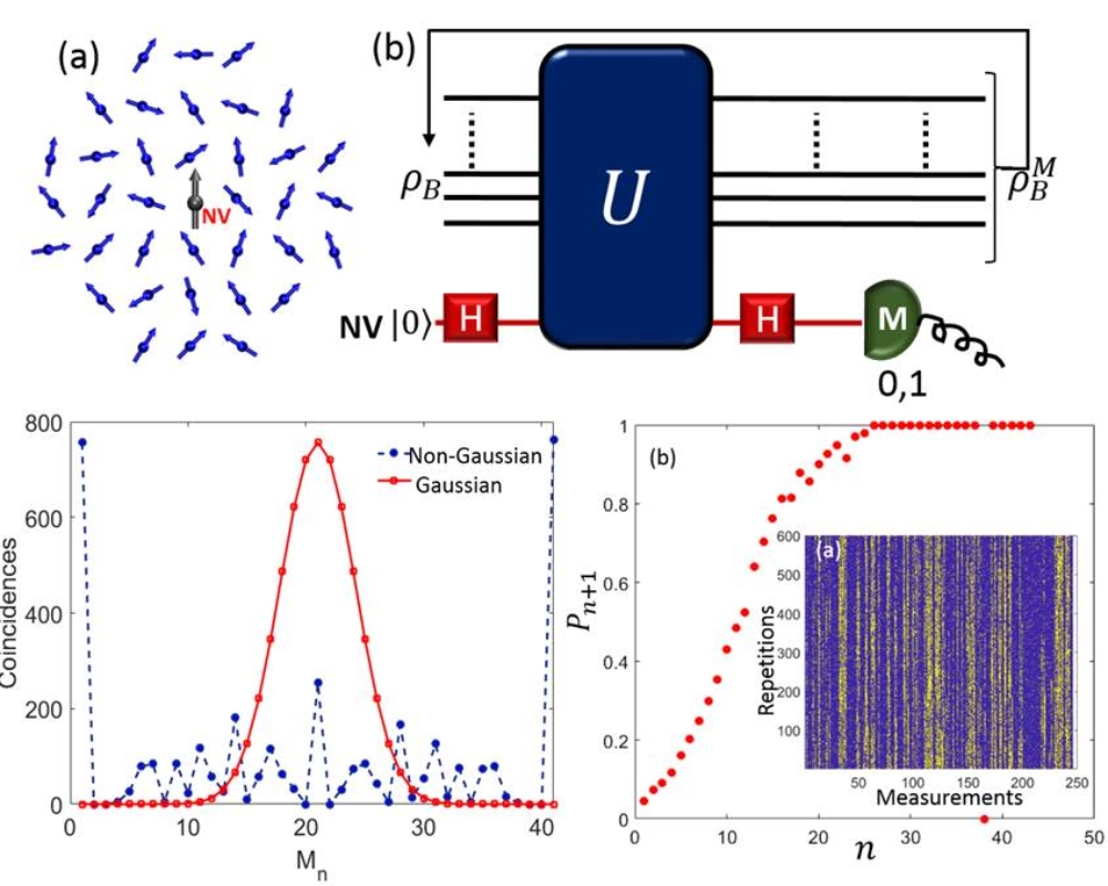
Highly efficient measurements are among the main pillars which modern quantum technology stands. A projective readout can allow for single shot experiments and to initialise the system by measurements. However in reality the intrinsic decay of the system perturbs the state during the readout.
The analysis of initialisation fidelity performed by such measurement is usually done either empirically or using some assumptions.
In recent paper we provide an analytical model which provides accurate estimation of post selection fidelity and verify it experimentally using three most common photon counting readouts, such as charge state, low temperature resonant excitation readout and nuclear spin assisted readout.
References:
Majid Zahedian, Max Keller, Minsik Kwon, Javid Javadzade, Jonas Meinel, Vadim Vorobyov and Jörg Wrachtrup, Published 19 December 2023, , ,

Charge state instabilities have been a bottleneck for the implementation of solid-state spin systems and pose a major challenge to the development of spin-based quantum technologies. In this publication we investigate the stabilization of negatively charged nitrogen-vacancy (NV−) centers in phosphorus-doped diamond at liquid helium temperatures. Photoionization of phosphorous donors in conjunction with charge diffusion at the nanoscale enhances NV0 to NV− conversion and stabilizes the NV− charge state without the need for an additional repump laser. The phosphorus-assisted stabilization is explored and confirmed both with experiments and our theoretical model. Stable photoluminescence-excitation spectra are obtained for NV− centers created during the growth. The fluorescence is continuously recorded under resonant excitation to real-time monitor the charge state and the ionization and recombination rates are extracted from time traces. We find a linear laser power dependence of the recombination rate as opposed to the conventional quadratic dependence, which is attributed to the photo-ionization of phosphorus atoms.
Publication:
Dopant-assisted stabilization of negatively charged single nitrogen-vacancy centers in phosphorus-doped diamond at low temperatures; Jianpei Geng, Tetyana Shalomayeva, Mariia Gryzlova, Amlan Mukherjee, Santo Santonocito, Dzhavid Dzhavadzade, Durga Bhaktavatsala Rao Dasari, Hiromitsu Kato, Rainer Stöhr, Andrej Denisenko, Norikazu Mizuochi & Jörg Wrachtrup; npj Quantum Information volume 9, Article number: 110 (2023)
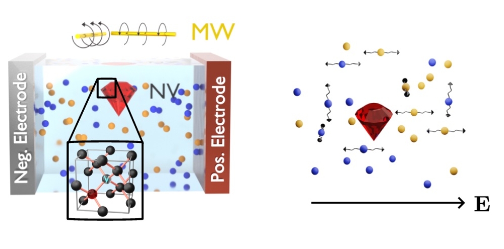
To use batteries as large-scale energy storage systems it is necessary to measure and understand their degradation in-situ and in-operando. As a battery’s degradation is often the result of molecular processes inside the electrolyte, a sensing platform which allows to measure the ions with a high spatial resolution is needed. Using NV centers we were able to deduce the electric field distribution and propose a protocol, which allows to characterize the battery’s state of charge and to obtain insight into the transport processes happening inside the electrolyte, like for instance diffusion.
References:
M. Hollendonner, S. Sharma, S. K. Parthasarathy, D. B. R. Dasari, A. Finkler, S. V. Kusminskiy and R. Nagy, New J. Phys. 25 (2023) 093008
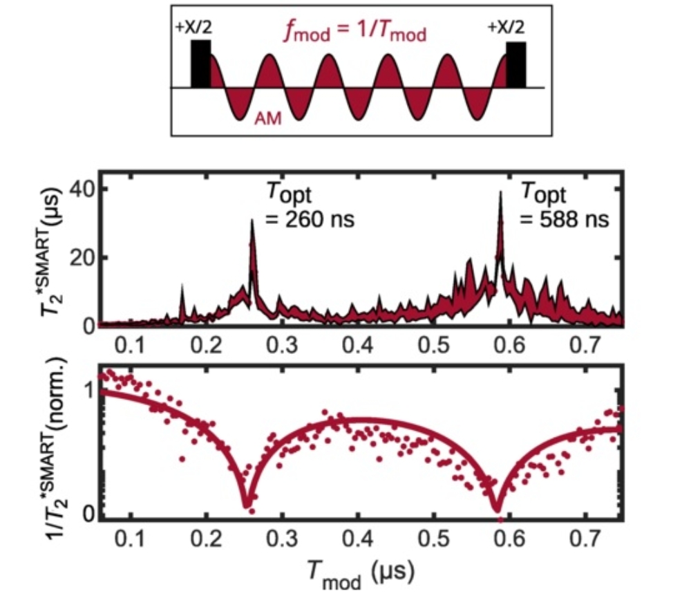
We show how the sinusoidally modulated, always rotating, and tailored (SMART) protocol, an extension of the dressed-qubit concept, can be implemented for continuous protection to offer Clifford gate fidelities compatible with fault-tolerant schemes, whilst prolonging the coherence time of a single NV− qubit at room temperature. We show an improvement in the average Clifford gate fidelity from 0.940±0.005 for the bare qubit to 0.993±0.002 for the SMART qubit, with the nitrogen nuclear spin in a random orientation. We further show a ≳30 times improvement in the qubit T∗2 coherence times compared to the bare qubit. This work paves the way for a practical implementation of a quantum computer that requires robust qubits that are protected against their noisy environment.
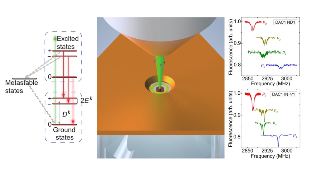
High-pressure experiments are crucial in modern interdisciplinary research fields such as engineering quantum materials, yet local probing techniques remain restricted due to the tight confinement of the pressure chamber in certain pressure devices. Recently, the negatively charged nitrogen-vacancy (N-V) center has emerged as a robust and versatile quantum sensor in pressurized environments. There are two popular ways to implement N-V sensing in a diamond anvil cell (DAC), which is a conventional workhorse in the high-pressure community: create implanted N-V centers (IN-Vs) at the diamond anvil tip or immerse N-V-enriched nanodiamonds (NDs) in the pressure medium. Nonetheless, there are limited studies on comparing the local stress environments experienced by these sensor types as well as their performances as pressure gauges. In this work, by probing the N-V energy levels with the optically detected magnetic resonance (ODMR) method, we experimentally reveal a dramatic difference in the partially reconstructed stress tensors of IN-Vs and NDs incorporated in the same DAC. Our measurement results agree with computational simulations, concluding that IN-Vs perceive a more nonhydrostatic environment dominated by a uniaxial stress along the DAC axis. This provides insights on the suitable choice of N-V sensors for specific purposes and the stress distribution in a DAC. We further propose some possible methods, such as using NDs and diamond nanopillars, to extend the maximum working pressure of quantum sensing based on ODMR spectroscopy, since the maximum working pressure could be restricted by nonhydrostaticity of the pressure environment. Moreover, we explore more sensing applications of the N-V center by studying how pressure modifies different aspects of the N-V system. We perform a PL study using both IN-Vs and NDs to determine the pressure dependence of the zero-phonon line, which helps developing an all-optical pressure sensing protocol with the N-V center. We also characterize the spin-lattice relaxation (T1) time of IN-Vs under pressure to lay a foundation for robust pulsed measurements with N-V centers in pressurized environments.
References:
Spectroscopic Study of N-V Sensors in Diamond-Based High-Pressure Devices
Kin On Ho, Man Yin Leung, Wenyan Wang, Jianyu Xie, King Yau Yip, Jiahao Wu, Swee K. Goh, Andrej Denisenko, Jörg Wrachtrup, and Sen Yang; Phys. Rev. Applied 19, 044091
The work in the publication
Transition from quantum to classical dynamics in weak measurements and reconstruction of quantum correlation
Vadim V. Vorobyov, Jonas Meinel, Hitoshi Sumiya, Shinobu Onoda, Junichi Isoya, Oleg Gulinsky, and Jörg Wrachtrup in the Physical Review A 107, 042212, published in April 2023
summarizes the recent experimental and theoretical progress in understanding quantum measurements with spin systems such as NV and aims at an analytical description of the underlying dynamics.
In a nutshell, it accurately describes how quantum sensors work and extract information about a quantum object that causes a back-action, using two spins as an example. We used the NV center in diamond with a single weakly coupled spin 13C located at a magic angle.
Possible outcomes of this work are ways to improve color center quantum hardware through continuous monitoring and quantum feedback, as well as next generation quantum sensing algorithms.
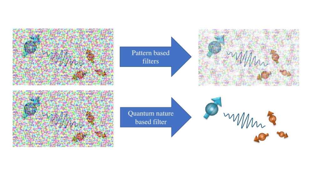
Extracting useful signals is key to both classical and quantum technologies. Conventional noise filtering methods rely on different patterns of signal and noise in frequency or time domains, thus limiting their scope of application, especially in quantum sensing. Here, we propose a signal-nature-based (not signal-pattern-based) approach which singles out a quantum signal from its classical noise background by employing the intrinsic quantum nature of the system. We design a novel protocol to extract the quantum correlation signal and use it to single out the signal of a remote nuclear spin from its overwhelming classical noise backgrounds, which is impossible to be accomplished by conventional filter methods. Our Letter demonstrates the quantum or classical nature as a new degree of freedom in quantum sensing. The further generalization of this quantum nature-based method opens a new direction in quantum research.
References:
Yang Shen, Ping Wang, Chun Tung Cheung, Jörg Wrachtrup, Ren-Bao Liu and Sen Yang
Phys. Rev. Lett. 130, 070802 – Published 17 February 2023
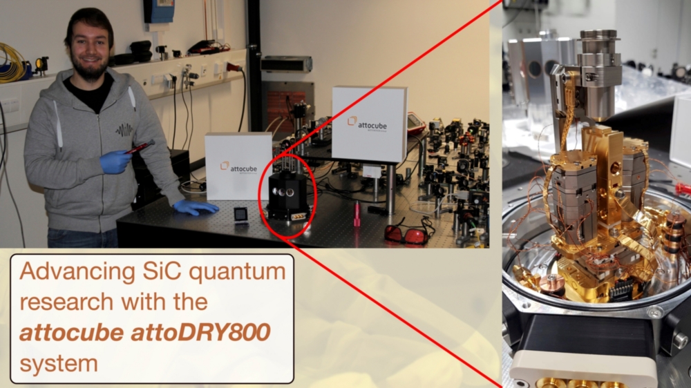
PhD candidate Timo Steidl from the 3rd Physics Institute has happily received a new custom-design closed-cycle optical cryostat system from attocube systems AG, our collaboration partner in the InQuRe project (Horizon 2020, Grant Agreement no. 731473 and 101017733).
The cryostat reaches a sample temperature of 4.0 K with <15 mK stability, while providing an extremely large sample chamber (130mm diameter, 150mm height) and low vibration levels. Together with attocube engineers, we have pushed the boundaries of system integration. Our cryostat now features 9 piezo-positioners (open- and closed-loop operation), 2 optical fibre feedthroughs (upgradable to 6), 3 microwave feedthroughs (upgradable to 6), as well as 6 pairs of twisted cables for low-power control.
All optical components (windows, objective) have been optimized for the wavelength range 900 – 1200 nm to facilitate our work with silicon vacancy colour centres (VSi) in silicon carbide (SiC).
Using this cryostat system, Timo Steidl will pursue his work towards increasing the scalability of VSi centres in SiC, e.g., as required for distributed quantum computing architectures. Some of the experiments that we will implement in this system are:
- Control and spectral stability improvement of VSi centres in SiC p-i-n diodes.
- Wavelength tuning of individual VSi centres with strain and electric fields.
- Photonic interference experiments based on multiple VSi centres in different fibre coupled SiC waveguides.
We are very optimistic that this system will allow us to make the necessary steps towards distributed quantum computing based on SiC colour centres.
Single color centers in solid have emerged as promising physical platforms for quantum information science. Creating these centers with excellent quantum properties is a key foundation for further technological developments. In particular, the microscopic understanding of the spin-bath environments is the key to engineer color centers for quantum control. In this work, we propose and demonstrate a distinct high-temperature annealing (HTA) approach for creating high-quality nitrogen vacancy (N-V) centers in implantation-free diamonds. Simultaneously using the created N-V centers as probes for their local environment we verify that no damage is microscopically induced by the HTA. Nearly all single N-V centers created in ultralow-nitrogen-concentration membranes possess stable and Fourier-transform-limited optical spectra. Furthermore, HTA strongly reduces noise sources naturally grown in ensemble samples, and leads to more than threefold improvements of decoherence time and sensitivity. We also verify that the vacancy activation and defect reformation, especially H3 and P1 centers, can explain the reconfiguration between spin baths and color centers. This distinct approach will become a powerful tool in vacancy-based quantum technology.
References:
King Cho Wong, San Lam Ng, Kin On Ho, Yang Shen, Jiahao Wu, Kwing To Lai, Man Yin Leung, Wai Kuen Leung, Durga Bhaktavatsala Rao Dasari, Andrej Denisenko, Jörg Wrachtrup, and Sen Yang
Phys. Rev. Applied 18, 024044 – Published 16 August 2022
The quantum Zeno and anti-Zeno paradigms have thus far addressed the evolution control of a quantum system coupled to an immutable bath via non-selective measurements performed at appropriate intervals. We fundamentally modify these paradigms by introducing, theoretically and experimentally, the concept of controlling the bath state via selective measurements of the system (a qubit). We show that at intervals corresponding to the anti-Zeno regime of the system-bath exchange, a sequence of measurements has strongly correlated outcomes. These correlations can dramatically enhance the bath-state purity and yield a low-entropy steady state of the bath. The purified bath state persists long after the measurements are completed. Such purification enables the exploitation of spin baths as long-lived quantum memories or as quantum-enhanced sensors. The experiment involved a repeatedly probed defect center dephased by a nuclear spin bath in a diamond at low-temperature.
References:
Anti-Zeno purification of spin baths by quantum probe measurements; Durga Bhaktavatsala Rao Dasari, Sen Yang, Arnab Chakrabarti, Amit Finkler, Gershon Kurizki & Jörg Wrachtrup; Nature Communications volume 13, Article number: 7527 (2022)
Quantum sensors are known for their high sensitivity in sensing applications. However, this sensitivity often comes with severe restrictions on other parameters which are also important. Examples are that in measurements of arbitrary signals, limitation in linear dynamic range could introduce distortions in magnitude and phase of the signal. High frequency resolution is another important feature for reconstructing unknown signals. In this publication, we demonstrate a distortion-free quantum sensing protocol that combines a quantum phase-sensitive detection with heterodyne readout. We present theoretical and experimental investigations using nitrogen-vacancy centers in diamond, showing the capability of reconstructing audio frequency signals with an extended linear dynamic range and high frequency resolution. Melody and speech based signals are used for demonstrating the features. The methods could broaden the horizon for quantum sensors towards applications, e.g. telecommunication in challenging environment, where low-distortion measurements are required at multiple frequency bands within a limited volume.
References:
Quantum-assisted distortion-free audio signal sensing, Chen Zhang, Durga Dasari, Matthias Widmann, Jonas Meinel, Vadim Vorobyov, Polina Kapitanova, Elizaveta Nenasheva, Kazuo Nakamura, Hitoshi Sumiya, Shinobu Onoda, Junichi Isoya & Jörg Wrachtrup, Nature Communications volume 13, Article number: 4637 (2022)
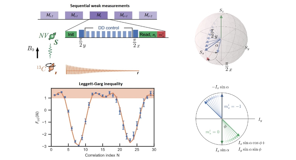
Towards high performance quantum technologies the understanding of qubit decoherence and correlations of fluctuations is paramount. Especially, higher order correlations give insights in the dynamics of quantum many-body systems and stochastic noise processes, as they suppress Gaussian noise while remaining sensitivity to non-linear signals. We extract high order correlations from a series of weak measurements of the target nuclear spin system. The quantumness and non-linearity of our sensor spin drives the target nuclear spin dynamics creating quantum and classical fourth order correlations. Experimentally, we measure high order correlations of a single nuclear spin and radio frequency magnetic fields with the nitrogen vacancy center in diamond. Quantum non-linear spectroscopy allows us to distinguish the 13C nuclear spin precession signal from the radio frequency signal via finger prints features in the high order spectra. Further the nuclear spin signal can originate from many nuclear spins N, which we can determine qualitatively and quantitatively through high order correlations. Quantum correlations scale with N while classical scale with N2, expressed as (1 – 1/N ), analogous to a g(2) photon correlation measurement. This work constitutes an initial step toward the application of higher-order correlations to quantum sensing. It may be used in future to examine the quantum foundation (by, e.g., higher-order Leggett-Garg inequality) and to study quantum many-body physics.
References:
Quantum nonlinear spectroscopy of single nuclear spins, Jonas Meinel, Vadim Vorobyov, Ping Wang, Boris Yavkin, Mathias Pfender, Hitoshi Sumiya, Shinobu Onoda, Junichi Isoya, Ren-Bao Liu & J. Wrachtrup, Nature Communications volume 13, Article number: 5318 (2022)
The performance of qubit-based technologies can be strongly limited by environmental sources of noise and disorder that cause decoherence. Qubits used in quantum sensing are usually very close to the host surface to enhance their coupling to external targets. This leaves them vulnerable to the effects of the surrounding noisy electron spin bath near the surface, which is very challenging to eliminate. Here we developed an efficient method to engineer the immediate electrostatic environment of nitrogen vacancy centre qubits located several nanometres beneath the diamond surface. We adopt a ‘pull-and-push’ strategy for near-surface charge manipulation using the strong local electric field of an atomic force microscope tip. Our technique is particularly effective for extremely shallow nitrogen vacancy centres, increasing their spin echo time by up to 20 fold. This corresponds to an 80-fold enhancement in the potential sensitivity for detecting individual external proton spins. Our work not only represents a step towards overcoming a fundamental restriction to applications of shallow nitrogen vacancy centres for quantum sensing but may also provide a general route for enhancing the coherence of solid-state qubits.
References:
Coherence enhancement of solid-state qubits by local manipulation of the electron spin bath; Wentian Zheng, Ke Bian, Xiakun Chen, Yang Shen, Shichen Zhang, Rainer Stöhr, Andrej Denisenko, Jörg Wrachtrup, Sen Yang & Ying Jiang; Nature Physics (2022)

We investigate, theoretically and experimentally, the thermodynamic performance of a minimal three-qubit heat-bath algorithmic cooling refrigerator. We analytically compute the coefficient of performance, the cooling power, and the polarization of the target qubit for an arbitrary number of cycles, taking realistic experimental imperfections into account. We determine their fundamental upper bounds in the ideal reversible limit and show that these values may be experimentally approached using a system of three qubits in a nitrogen-vacancy center in diamond.
References:
Thermodynamics of a Minimal Algorithmic Cooling Refrigerator
Rodolfo R. Soldati, Durga B. R. Dasari, Jörg Wrachtrup, and Eric Lutz, Phys. Rev. Lett. 129, 030601 (2022)
Color centers in silicon carbide are emerging candidates for distributed spin-based quantum applications due to the scalability of host materials and the demonstration of integration into nanophotonic resonators. Recently, silicon vacancy centers in silicon carbide have been identified as a promising system with excellent spin and optical properties.
Here, we fully study the spin-optical dynamics of the single silicon vacancy center at hexagonal lattice sites, namely V1, in 4H-polytype silicon carbide. By utilizing resonant and above-resonant sublifetime pulsed excitation, we determine spin-dependent excited-state lifetimes and intersystem-crossing rates. Our new approach to inferring the intersystem-crossing rates is based on all-optical pulsed initialization and readout scheme, and is applicable to spin-active color centers with similar dynamics models. In addition, the optical transition dipole strength and the quantum efficiency of V1 defect are evaluated based on coherent optical Rabi measurement and local-field calibration employing electric field simulation. With our model, we can now fully explain spin-state polarization dynamics and determine optimal pulse sequences for quantum sensing protocols.
Additionally, we outline optimal pathways towards improving the photoemission dynamics in resonant enhancement structures, such as required in quantum networks based on optically connected silicon vacancy centers in silicon carbide.
References:
Spin-optical dynamics and quantum efficiency of a single V1 center in silicon carbide; Naoya Morioka, Di Liu, Öney O. Soykal, Izel Gediz, Charles Babin, Rainer Stöhr, Takeshi Ohshima, Nguyen Tien Son, Jawad Ul-Hassan, Florian Kaiser, and Jörg Wrachtrup, Physical Review Applied 17, 054005 (2022)
Electro-optical control of on-chip photonic devices is an essential tool for efficient integrated photonics. Lithium niobate on insulator (LNOI) is an emerging platform for on-chip photonics due to its large electro-optic coefficient and high nonlinearity. Integrating quantum emitters into LNOI would extend their versatility in classic photonics to quantum computing and communication. Here, we incorporate rare-earth ion (REI) quantum emitters into electro-optical tunable lithium niobite (LN) thin films and demonstrate control of LN microcavities coupled to REIs over a frequency range of 160 GHz with 5 µs switching speed. Dynamic control of the cavities enables modulation of the Purcell enhancement of REIs with short time constants. Using Purcell enhancement, we show evidence of detecting single Yb3+ions in LN cavities. Coupling quantum emitters in fast tunable photonic devices is an efficient method to shape the waveform of the emitter. It also offers a platform to encode quantum information in the integration of a spectral–temporal–spatial domain to achieve high levels of channel multiplexing, as well as an approach to generate deterministic single-photon sources.
References:
Tunable microcavities coupled to rare-earth quantum emitters; Kangwei Xia, Fiammetta Sardi, Colin Sauerzapf, Thomas Kornher, Hans-Werner Becker, Zsolt Kis, Laszlo Kovacs, Denis Dertli, Jonas Foglszinger, Roman Kolesov, and Jörg Wrachtrup, Optica Vol. 9, Issue 4, pp. 445-450 (2022)
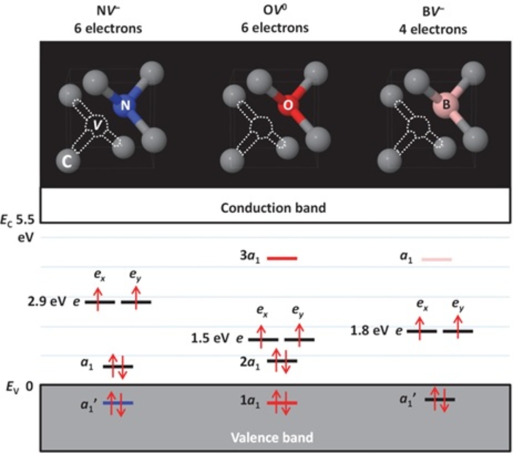
Impurity-vacancy complexes in diamond are an attractive family of spin defects since NV –, SiV –, GeV –, and SnV – have emerged as promising platforms for quantum applications. Although boron is most easily incorporated into diamond, a boron-vacancy complex in the negative charge state (BV –) has eluded experimental observation. This center was theoretically predicted as another promising spin qubit. In this work, we experimentally observed an electron paramagnetic resonance (EPR) spectrum identified as BV – in synthetic diamonds via a Fermi-level tuning. Fingerprints of BV – such as the spin multiplicity f S = 1, C3v symmetry, and the zero-field splitting (D = 2913 MHz), in addition to 10B and 11B hyperfine (HF) interactions, have been confirmed. Moreover, optically pumped spin polarization has been observed with 3.0–3.6 eV excitation. However, unlike the NV – center, the photoluminescence as well as optically detected magnetic resonance from BV – have not been confirmed even at low temperatures.We speculate that the Jahn-Teller instability in the triplet excited states of the NV – and BV – centers results in different optical properties.
References:
Negatively charged boron vacancy center in diamond
Phys. Rev. B 105, 165201 – Published 4 April 2022 – T. Umeda, K. Watanabe, H. Hara, H. Sumiya, S. Onoda, A. Uedono, I. Chuprina, P. Siyushev, F. Jelezko, J. Wrachtrup, and J. Isoya
Nuclei surrounding single electron spins are valuable resources for quantum technology. For application in this area, one is often interested in weakly coupled nuclei with coupling strength on the order of a few 10–100 kHz. In this paper, we compare methods to address single nuclear spins with this type of hyperfine coupling to a single electron spin. To achieve the required spectral resolution, we specifically focus on two methods, namely dynamical decoupling and correlation spectroscopy. We demonstrate spectroscopy of two single nuclear spins and present a method to derive components of their hyperfine coupling tensor from those measurements.
References:
Addressing Single Nuclear Spins Quantum Memories by a Central Electron Spin; V. Vorobyov, J. Javadzade, M. Joliffe, F. Kaiser & J. Wrachtrup, Applied Magnetic Resonance (2022)
Moiré superlattices of twisted nonmagnetic two-dimensional (2D) materials are highly controllable platforms for the engineering of exotic correlated and topological states. Here, we report emerging magnetic textures in small-angle twisted 2D magnet chromium triiodide (CrI3). Using single-spin quantum magnetometry, we directly visualized nanoscale magnetic domains and periodic patterns, a signature of moiré magnetism, and measured domain size and magnetization. In twisted bilayer CrI3, we observed the coexistence of antiferromagnetic (AFM) and ferromagnetic (FM) domains with disorder-like spatial patterns. In twisted double-trilayer CrI3, AFM and FM domains with periodic patterns appear, which is in good agreement with the calculated spatial magnetic structures that arise from the local stacking-dependent interlayer exchange interactions in CrI3 moiré superlattices. Our results highlight magnetic moiré superlattices as a platform for exploring nanomagnetism.
References:
Tiancheng Song, Qi-Chao Sun, Eric Anderson, Chong Wang, Jimin Qian, Takashi Taniguchi, Kenji Watanabe, Michael A McGuire, Rainer Stöhr, Di Xiao, Ting Cao, Jörg Wrachtrup, Xiaodong Xu, Science 374, 1140-1144 (2021)
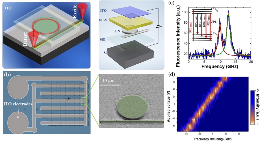
A promising route towards larger quantum computers is to orchestrate multiple task-optimised smaller systems. To dynamically connect and entangle any two systems, photonic interference emerges as a powerful method, due to its compatibility with on-chip devices and long-distance propagation in quantum networks.
In our recent work, published in Nature Materials, we showed that silicon vacancy (VSi) colour centres in silicon carbide (SiC) can reach these goals.
Our work followed a two-step approach. First, VSi centres in SiC are particularly robust quantum systems to start with. Second, we fabricated nanophotonic waveguides around VSi centres using gentle processing methods that keep the host material essentially free of damage.
With these techniques, we showed for the first time that waveguide-integrated colour centres can maintain, at the same time, life-time limited optical absorption lines, long spin coherence times (Hahn echo, 1.4 ms), as well as coherent access to nuclear spin qubits with fidelities exceeding 90%.
Our next steps target high-efficiency light collection via direct waveguide-to-fibre coupling, as well as maximising electrical control to independently tune multiple VSi centres on a complex photonic chip.
References:
Fabrication and nanophotonic waveguide integration of silicon carbide colour centres with preserved spin-optical coherence; Charles Babin, Rainer Stöhr, Naoya Morioka, Tobias Linkewitz, Timo Steidl, Raphael Wörnle, Di Liu, Erik Hesselmeier, Vadim Vorobyov, Andrej Denisenko, Mario Hentschel, Christian Gobert, Patrick Berwian, Georgy V. Astakhov, Wolfgang Knolle, Sridhar Majety, Pranta Saha, Marina Radulaski, Nguyen Tien Son, Jawad Ul-Hassan, Florian Kaiser & Jörg Wrachtrup; Nature Materials (2021)
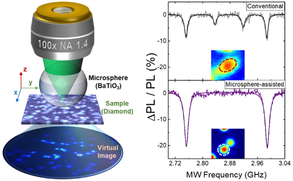
Point defects in crystals provide important building blocks for quantum applications. Since we optically address these defect qubits, having an efficient optical interface is a highly important aspect. However, conventional confocal fluorescence microscopy of high-refractive-index crystals suffers from limited photon collection efficiency and spatial resolution. Here, we demonstrate high-resolution, high-contrast imaging of defects in diamonds using microsphere-assisted confocal microscopy. A microsphere provides an excellent optical interface for point defects with a magnified virtual image that increases the spatial resolution up to lambda/5, as well as the optical signal-to-noise ratio by four times. These features enable individual optical addressing of single photons and single spins of multiple defects that are spatially unresolved in conventional confocal microscopy, with improved signal contrast. Combined with optical tweezers, this system also demonstrates the possibility of positioning or scanning the microspheres. The approach does not require any complicated fabrication or additional optical systems, but uses simple, off-the-shelf micro-optics. From these distinctive advantages of microspheres, our approach provides an efficient way to image and address closely spaced defects with much better resolution and sensitivity.
References:
High-Resolution, High-Contrast Optical Interface for Defect Qubits, Jong Sung Moon, Haneul Lee, Jin Hee Lee, Woong Bae Jeon, Dowon Lee, Junghyun Lee, Seoyoung Paik, Sang-Wook Han, Rolf Reuter, Andrej Denisenko, Jörg Wrachtrup, Sang-Yun Lee, and Je-Hyung Kim, ACS Photonics 2021, 8, 9, 2642–2649, August 19, 2021
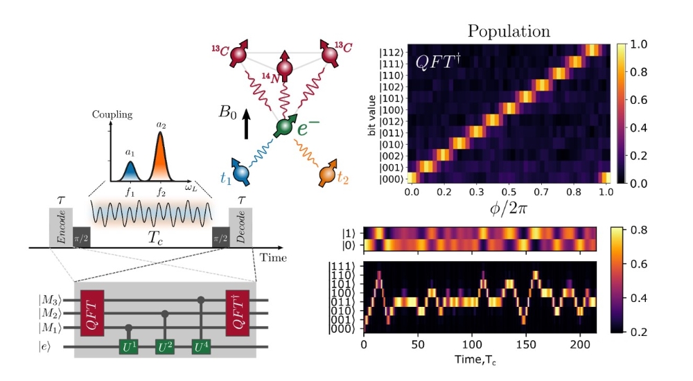
The quantum Fourier transformation (QFT) is a key building block for a whole wealth of quantum algorithms. Despite its proven efficiency, only a few proof-of-principle demonstrations have been reported. Here we utilize QFT to enhance the performance of a quantum sensor. We implement the QFT algorithm in a hybrid quantum register consisting of a nitrogen-vacancy (NV) center electron spin and three nuclear spins. The QFT runs on the nuclear spins and serves to process the sensor - i.e., the NV electron spin signal. Specifically, we show the application of QFT for correlation spectroscopy, where the long correlation time benefits the use of the QFT in gaining maximum precision and dynamic range at the same time. We further point out the ability for demultiplexing the nuclear magnetic resonance (NMR) signals using QFT and demonstrate precision scaling with the number of used qubits. Our results mark the application of a complex quantum algorithm in sensing which is of particular interest for high dynamic range quantum sensing and nanoscale NMR spectroscopy experiments.
References:
Quantum Fourier transform for nanoscale quantum sensing; Vadim Vorobyov, Sebastian Zaiser, Nikolas Abt, Jonas Meinel, Durga Dasari, Philipp Neumann & Jörg Wrachtrup; npj Quantum Information volume 7, Article number: 124 (2021)

The achievable bounds of cooling quantum systems, and the possibility to violate them is not well-explored experimentally. For example, among the common methods to enhance spin polarization (cooling), one utilizes the low temperature and high-magnetic field condition or employs a resonant exchange with highly polarized spins. The achievable polarization, in such cases, is bounded either by Boltzmann distribution or by energy conservation. Heat-bath algorithmic cooling schemes (HBAC), on the other hand, have shown the possibility to surpass the physical limit set by the energy conservation and achieve a higher saturation limit in spin cooling. Despite, the huge theoretical progress, and few principle demonstrations, neither the existence of the limit nor its application in cooling quantum systems towards the maximum achievable limit have been experimentally verified. Here, we show the experimental saturation of the HBAC limit for single nuclear spins, beyond any available polarization in solid-state spin system, the Nitrogen-Vacancy centers in diamond. We benchmark the performance of our experiment over a range of variable reset polarizations (bath temperatures), and discuss the role of quantum coherence in HBAC.
References:
Cyclic cooling of quantum systems at the saturation limit; Sebastian Zaiser, Chun Tung Cheung, Sen Yang, Durga Bhaktavatsala Rao Dasari, Sadegh Raeisi & Jörg Wrachtrup; npj Quantum Information volume 7, Article number: 92 (2021)
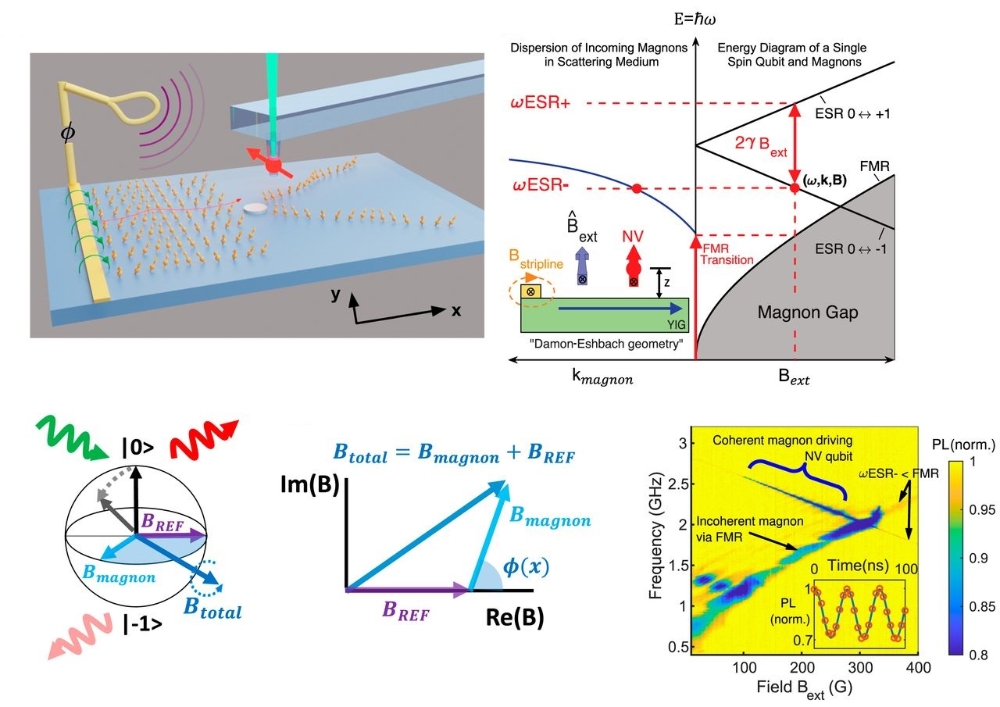
Scattering experiments have revolutionized our understanding of nature. Examples include the discovery of the nucleus [R. G. Newton, Scattering Theory of Waves and Particles (1982)], crystallography [U. Pietsch, V. Holý, T. Baumback, High-Resolution X-Ray Scattering (2004)], and the discovery of the double-helix structure of DNA [J. D. Watson, F. H. C. Crick, Nature 171, 737–738]. Scattering techniques differ by the type of particles used, the interaction these particles have with target materials, and the range of wavelengths used. Here, we demonstrate a two-dimensional table-top scattering platform for exploring magnetic properties of materials on mesoscopic length scales. Long-lived, coherent magnonic excitations are generated in a thin film of yttrium iron garnet and scattered off a magnetic target deposited on its surface. The scattered waves are then recorded using a scanning nitrogen vacancy center magnetometer that allows subwavelength imaging and operation under conditions ranging from cryogenic to ambient environment. While most scattering platforms measure only the intensity of the scattered waves, our imaging method allows for spatial determination of both amplitude and phase of the scattered waves, thereby allowing for a systematic reconstruction of the target scattering potential. Our experimental results are consistent with theoretical predictions for such a geometry and reveal several unusual features of the magnetic response of the target, including suppression near the target edges and a gradient in the direction perpendicular to the direction of surface wave propagation. Our results establish magnon scattering experiments as a platform for studying correlated many-body systems.
References:
A magnon scattering platform, Tony X. Zhou, Joris J. Carmiggelt, Lisa M. Gächter, Ilya Esterlis, Dries Sels, Rainer J. Stöhr, Chunhui Du, Daniel Fernandez, Joaquin F. Rodriguez-Nieva, Felix Büttner, Eugene Demler, and Amir Yacoby,
PNAS June 22, 2021 118 (25) e2019473118
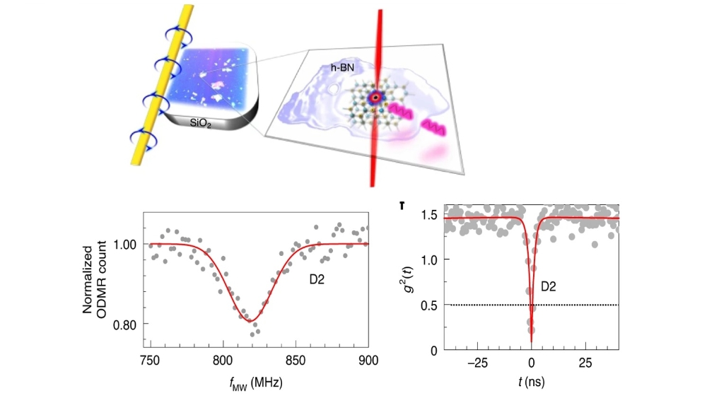
A plethora of single-photon emitters have been identified in the atomic layers of two-dimensional van der Waals materials. Here, we report on a set of isolated optical emitters embedded in hexagonal boron nitride that exhibit optically detected magnetic resonance. The defect spins show an isotropic ge-factor of ~2 and zero-field splitting below 10 MHz. The photokinetics of one type of defect is compatible with ground-state electron-spin paramagnetism. The narrow and inhomogeneously broadened magnetic resonance spectrum differs significantly from the known spectra of in-plane defects. We determined a hyperfine coupling of ~10 MHz. Its angular dependence indicates an unpaired, out-of-plane delocalized π-orbital electron, probably originating from substitutional impurity atoms. We extracted spin–lattice relaxation times T1 of 13–17 μs with estimated spin coherence times T2 of less than 1 μs. Our results provide further insight into the structure, composition and dynamics of single optically active spin defects in hexagonal boron nitride.
References:
Single-spin resonance in a van der Waals embedded paramagnetic defect; Nathan Chejanovsky, Amlan Mukherjee, Jianpei Geng, Yu-Chen Chen, Youngwook Kim, Andrej Denisenko, Amit Finkler, Takashi Taniguchi, Kenji Watanabe, Durga Bhaktavatsala Rao Dasari, Philipp Auburger, Adam Gali, Jurgen H. Smet & Jörg Wrachtrup, Nature Materials (2021), 06 May 2021
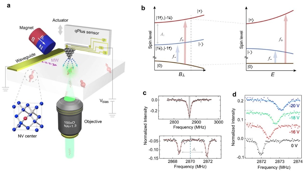
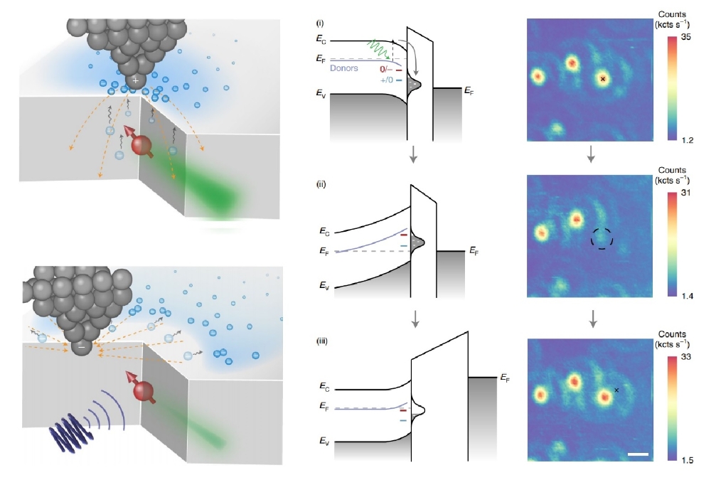
Nitrogen-vacancy (NV) centers in diamond can be used as quantum sensors to image the magnetic field with nanoscale resolution. However, nanoscale electric-field mapping has not been achieved so far because of the relatively weak coupling strength between NV and electric field. Here, using individual shallow NVs, we quantitatively image electric field contours from a sharp tip of a qPlus-based atomic force microscope (AFM), and achieve a spatial resolution of ~10 nm. Through such local electric fields, we demonstrated electric control of NV’s charge state with sub-5 nm precision. This work represents the first step towards nanoscale scanning electrometry based on a single quantum sensor and may open up the possibility of quantitatively mapping local charge, electric polarization, and dielectric response in a broad spectrum of functional materials at nanoscale.
References:
Nanoscale electric-field imaging based on a quantum sensor and its charge-state control under ambient condition
Ke Bian, Wentian Zheng, Xianzhe Zeng, Xiakun Chen, Rainer Stöhr, Andrej Denisenko, Sen Yang, Jörg Wrachtrup & Ying Jiang; Nature Communications volume 12, Article number: 2457 (2021)
The emergence of atomically thin van der Waals magnets provides a new platform for the studies of two-dimensional magnetism and its applications. However, the widely used measurement methods in recent studies cannot provide quantitative information of the magnetization nor achieve nanoscale spatial resolution. These capabilities are essential to explore the rich properties of magnetic domains and spin textures. Here, we employ cryogenic scanning magnetometry using a single-electron spin of a nitrogen-vacancy center in a diamond probe to unambiguously prove the existence of magnetic domains and study their dynamics in atomically thin CrBr3. By controlling the magnetic domain evolution as a function of magnetic field, we find that the pinning effect is a dominant coercivity mechanism and determine the magnetization of a CrBr3 bilayer to be about 26 Bohr magnetons per square nanometer. The high spatial resolution of this technique enables imaging of magnetic domains and allows to locate the sites of defects that pin the domain walls and nucleate the reverse domains. Our work highlights scanning nitrogen-vacancy center magnetometry as a quantitative probe to explore nanoscale features in two-dimensional magnets.
References:
Magnetic domains and domain wall pinning in atomically thin CrBr3 revealed by nanoscale imaging; Qi-Chao Sun, Tiancheng Song, Eric Anderson, Andreas Brunner, Johannes Förster, Tetyana Shalomayeva, Takashi Taniguchi, Kenji Watanabe, Joachim Gräfe, Rainer Stöhr, Xiaodong Xu & Jörg Wrachtrup; Nature Communications volume 12, Article number: 1989 (2021)
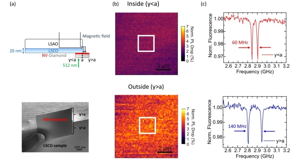
Microscopic studies on thin film superconductors play an important role for probing non-equilibrium phase transitions and revealing dynamics at the nanoscale. However, magnetic sensors with nanometer scale spatial and picosecond temporal resolution are essential for exploring these. Here, we present an all-optical, microwave-free method that utilizes the negatively charged nitrogen-vacancy (NV) center in diamond as a non-invasive quantum sensor and enables the spatial detection of the Meissner state in a superconducting thin film. We place an NV implanted diamond membrane on a 20 nm thick superconducting La2-xSrxCuO4 (LSCO) thin film with Tc of 34 K. The strong B-field dependence of the NV photoluminescence allows us to investigate the Meissner screening in LSCO under an externally applied magnetic field of 4.2 mT in a non-resonant manner. The magnetic field profile along the LSCO thin film can be reproduced using Brandt’s analytical model, revealing a critical current density jc of 1.4 x 10⁸ A/cm2. Our work can be potentially extended further with a combination of optical pump probe spectroscopy for the local detection of time-resolved dynamical phenomena in nanomagnetic materials.
References:
All-optical and microwave-free detection of Meissner screening using nitrogen-vacancy centers in diamond featured
Journal of Applied Physics 129, 024306 (2021); https://doi.org/10.1063/5.0037414, D. Paone, D. Pinto, G. Kim, L. Feng, M.-J. Kim, R. Stöhr, A. Singha, S. Kaiser, G. Logvenov, B. Keimer, J. Wrachtrup, and K. Kern
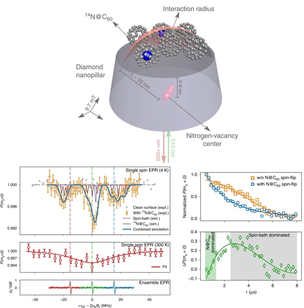
Atomic spins for quantum technologies need to be individually addressed and positioned with nanoscale precision. C60 fullerene cages offer a robust packaging for atomic spins, while allowing in-situ physical positioning at the nanoscale. However, achieving single-spin level readout and control of endofullerenes has so far remained elusive. In this work, we demonstrate electron paramagnetic resonance on an encapsulated nitrogen spin (14N@C60) within a C60 matrix using a single near-surface nitrogen vacancy (NV) center in diamond at 4.7 K. Exploiting the strong magnetic dipolar interaction between the NV and endofullerene electronic spins, we demonstrate radio-frequency pulse controlled Rabi oscillations and measure spin-echos on an encapsulated spin. Modeling the results using second-order perturbation theory reveals an enhanced hyperfine interaction and zero-field splitting, possibly caused by surface adsorption on diamond. These results demonstrate the first step towards controlling single endofullerenes, and possibly building large-scale endofullerene quantum machines, which can be scaled using standard positioning or self-assembly methods.
References:
Readout and control of an endofullerene electronic spin, Dinesh Pinto, Domenico Paone, Bastian Kern, Tim Dierker, René Wieczorek, Aparajita Singha, Durga Dasari, Amit Finkler, Wolfgang Harneit, Jörg Wrachtrup & Klaus Kern, Nature Communications 11, 6405 (2020).
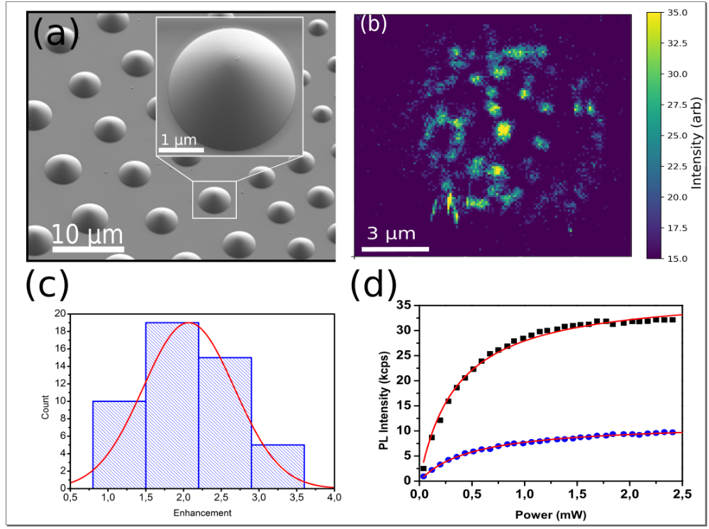
Silicon carbide (SiC) is an appealing material for quantum technologies and nanophotonics due to its optical transparency, and low nuclear spin bath. One species of promising quantum emitters found in the 4H-SiC polytype is the silicon vacancy defects VSi. It exhibits a long spin coherence time at room temperature and accessible coherence control of single spins. However, the high refractive index of the material leads to strong refraction and total internal reflection at the SiC-air interface, which results in reduction of the collected defects photoluminescence.
A possibility to circumvent this effect is the fabrication of shallow solid immersion lenses of a few micrometers in size on a SiC wafer, resulting in refractionless transmission of light through the SIL surface. A similar approach has already been proven to be advantageous for enhancing the fluorescence yield of nitrogen-vacancy (NV) centers in diamond or for studies in the spin properties of rare earth ions. Typically, SILs in diamond are fabricated by focused ion beam (FIB) milling. This approach is intrinsically time-consuming and unscalable. In addition, it leads to contamination of the surface of the SIL with gallium and damages the crystalline structure. Studies dealing with quantum-dots describe the scalable fabrication of lenses with a low NA of 0.4 and discussing the potential of high NA lenses with respect to collection efficiency. Also, previous work on scalable photonics for SiC dealt with nanopillars tailored to 0.65 NA for signal collection, potentially with lensed fiber arrays. With increasing NA of lensed fibers in experiments and theoretical proposals, a high NA collection of light in a scalable fashion comes into reach.
The experiment introduces a scalable, method of producing SILs capable to work with high NA objective by imprinting hemispherical droplets of a reflown photoresist onto the surface of SiC by plasma etching. The performance of the resulting SILs is evaluated by comparing the fluorescence collected from single VSi centers under the SIL with centers under a pristine SiC surface. The fluorescence collection efficiency of single quantum emitters under the SILs shows 3.4 times enhancement confirmed by confocal microscopy of individual V2.
References
Appl. Phys. Lett. 117, 022105 (2020); https://doi.org/10.1063/5.0011366
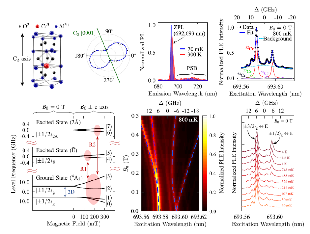
Paramagnetic ions in solid state crystals form the basis for many advanced technologies such as lasers, masers, frequency standards, and quantum-enhanced sensors. One of the most-studied examples is the Cr3+ ion in sapphire (Al2O3), also known as ruby, which has been intensely studied in the 1950s and 1960s. However, despite decades of research on ruby, some of its fundamental optical and spin properties have not yet been characterized at ultralow temperatures. In this paper, we present optical measurements on a ruby crystal in a dilution refrigerator at ultralow temperatures down to 20 mK. Analyzing the relative populations of its 4A2 ground-state spin levels, we extract a lattice temperature of 143±7mK under continuous laser excitation. We perform spin-lattice relaxation T1 measurements in excellent agreement with the direct, one-phonon model. Furthermore, we perform optically detected magnetic resonance measurements showing magnetically driven transitions between the ground-state spin levels for various magnetic fields. Our measurements characterize some of ruby's low-temperature spin properties, and lay the foundations for more advanced spin control experiments.
References
Spin thermometry and spin relaxation of optically detected Cr3+ ions in ruby Al2O3, Vikas K. Sewani, Rainer J. Stöhr, Roman Kolesov, Hyma H. Vallabhapurapu, Tobias Simmet, Andrea Morello, and Arne Laucht Phys. Rev. B 102, 104114 – Published 25 September 2020
In current long-distance communications, classical information can be eavesdropped without notice. On the other hand, quantum communications can provide provable privacy and could make use of entanglement swapping via quantum repeaters to mitigate transmission losses.
To reach this goal, considerable efforts have been spent over the last few decades toward developing quantum repeaters, notably in the solid-state. Multiple candidate optical spin qubits in the solid state, including quantum dots, rare-earth ions, and color centers in diamond and silicon carbide (SiC), have been developed.
In this perspective article, we summarize the latest advances in developing optically active spin qubits in SiC, and outline future research directions. Thanks to established semiconductor fabrication and processing techniques, we show that the SiC platform is highly promising to realize the targeted applications in quantum repeater networks.
References:
Appl. Phys. Lett. 116, 190501 (2020); https://doi.org/10.1063/5.0004454

The occurrence of any physical process is restricted by the constraints imposed by the laws of thermodynamics on the energy and entropy exchange involved. A prominent class of processes where thermodynamic constraints are crucial involve polarization of nuclear spin baths that are at the heart of magnetic resonance imaging (MRI), nuclear magnetic resonance (NMR), quantum information processing. Polarizing a spin bath, is the key to enhancing the sensitivity of these tools, leading to new analytical capabilities and improved medical diagnostics. In recent years, significant effort has been invested in identifying the far-reaching consequences of quantum modifications to classical thermodynamics for such processes. Here we focus on the adverse role of quantum correlations (entanglement) in the spin bath that can impede its cooling in many realistic scenarios. We propose to remove this impediment by modified cooling schemes, incorporating probe-induced disentanglement or, equivalently, alternating non-commuting probe–bath interactions to suppress the buildup of quantum correlations in the bath. The resulting bath polarization is thereby exponentially enhanced. The underlying quantum thermodynamic principles have far-reaching implications for a broad range of quantum technological applications.
References:
D. Durga Bhaktavatsala Rao Dasari, et. al. - Spin-bath polarization via disentanglement, New Journal of Physics (2020)
Machine learning (ML) has become an attractive tool for solving various problems in different fields of physics, including the quantum domain. Here, we show how classical reinforcement learning (RL) could be used as a tool for quantum state engineering (QSE). We employ a measurement based control for QSE where the action sequences are determined by the choice of the measurement basis and the reward through the fidelity of obtaining the target state. Our analysis clearly displays a learning feature in QSE, for example in preparing arbitrary two-qubit entangled states and delivers successful action sequences that generalise previously found human solutions from exact quantum dynamics. We provide a systematic algorithmic approach for using RL for quantum protocols that deal with a non-trivial continuous state space, and discuss the scaling of these approaches for the preparation of larger entangled (cluster) states.
References:
Jelena Mackeprang, Durga B. Rao Dasari & Jörg Wrachtrup
Quantum Machine Intelligence 2, 1–14(2020)
Quantum systems combining indistinguishable photon generation and spin-based quantum information processing are essential for remote quantum applications and networking. In our recent work, we use silicon vacancy centres in silicon carbide to demonstrate controlled emission of indistinguishable and distinguishable photons via coherent spin manipulation. Although using strong off-resonant excitation, the system’s exceptional spectral stability allows us to measure two-photon interference contrasts close to 90% in Hong-Ou-Mandel type experiments. We also exploit the system’s intimate spin-photon relation to spin-control the colour and indistinguishability of consecutively emitted photons. The resulting two-photon quantum beating at a frequency of 966 MHz is shown in the figure. These results prove that spin-photon entanglement generation and photonic cluster state production are achievable with the system.
Further, our temperature dependent studies provide a deep insight into the system’s spin-phonon-photon physics, underlining the potential of the industrially compatible silicon carbide platform.
Our future efforts will focus on realising spin-photon entanglement and utilising hyperfine coupling to nuclear spin quantum registers for single-shot spin readout and other high-level network-relevant quantum information processing protocols.
Reference: Naoya Morioka et al., Nature Communications 11, 2516 (2020)
The measurement of a single nuclear spin in a noisy spin environment opens up new possibilities for quantum technologies.
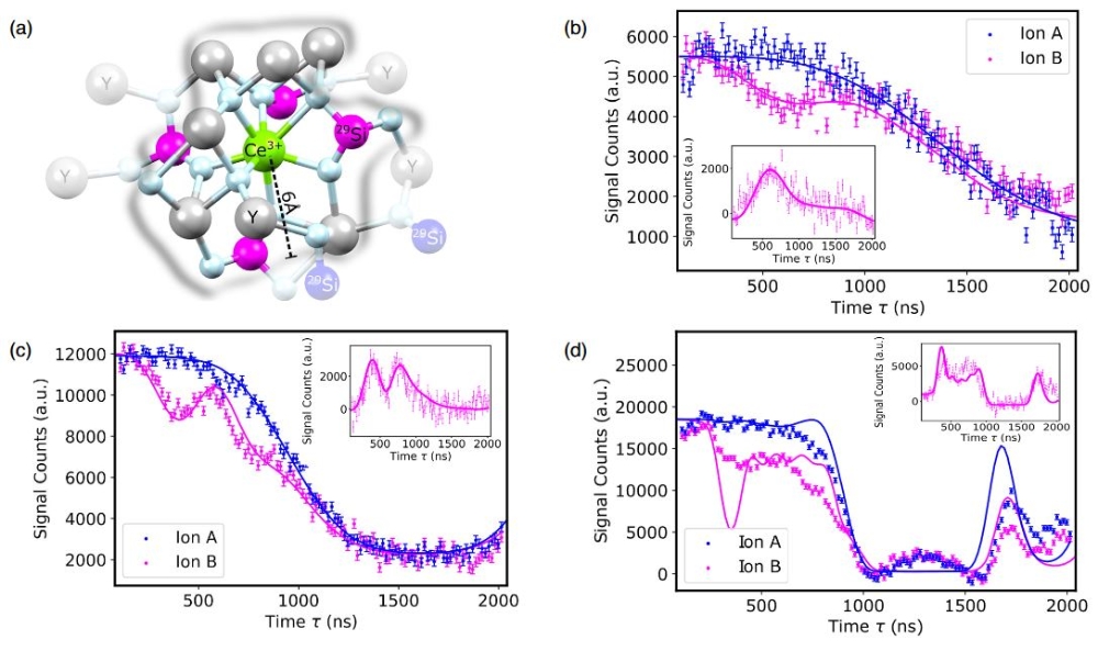
Rare-earth related electron spins in crystalline hosts are unique material systems, as they can potentially provide a direct interface between telecom band photons and long-lived spin quantum bits. Specifically, their optically accessible electron spins in solids interacting with nuclear spins in their environment are valuable quantum memory resources. Detection of nearby individual nuclear spins, so far exclusively shown for few dilute nuclear spin bath host systems such as the nitrogen-vacancy center in diamond or the silicon vacancy in silicon carbide, remained an open challenge for rare earths in their host materials, which typically exhibit dense nuclear spin baths. Here, we present the electron spin spectroscopy of single Ce3+ ions in a yttrium orthosilicate host, featuring a coherence time of T2=124 μs. This coherent interaction time is sufficiently long to isolate proximal 89Y nuclear spins from the nuclear spin bath of 89Y. Furthermore, it allows for the detection of a single nearby 29Si nuclear spin, native to the host material with ∼5% abundance. This study opens the door to quantum memory applications in rare-earth ion related systems based on coupled environmental nuclear spins, potentially useful for quantum error correction schemes.
This research is published in Physical Review Letters.
Review by Marric Stephens based in Bristol, UK "Sensing Single Spins in Dense Spin Baths" in Physics.
Sensing Individual Nuclear Spins with a Single Rare-Earth Electron Spin
Single rare-earth ions are hard to observe and even harder to use as qubits. However, with the help of coupling to an optical cavity and clever engineering of selection rules, a big step has been taken to establish their new role in the quantum world.
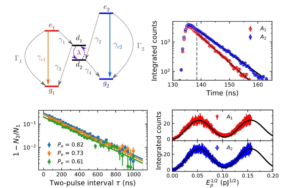
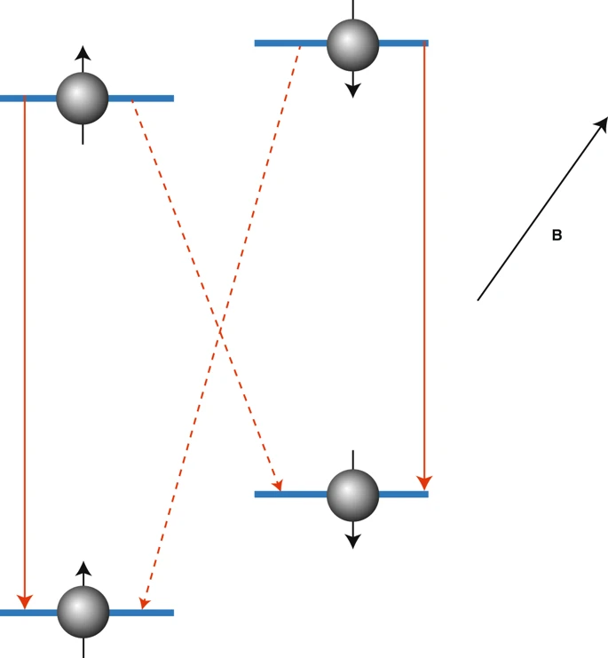
Rare-earth ions (REIs) in crystals are excellent candidates for optically addressable quantum memory. This is because of their optically active 4f electrons, shielded from environmental distortions by a Faraday cage comprised of filled 5s and 5p electron shells1. Record-long decoherence times of six hours have been demonstrated in an ensemble of europium doped into yttrium orthosilicate (YSO)2. However, to make REI-based quantum architectures fully scalable one has to address the ions at the level of single atoms. Now, writing in Nature Communications and Nature, respectively, Mouktik Raha and colleagues3 and Jonathan M. Kindem and colleagues4 have not only reported the detection of individual REIs, but also implemented a protocol for single shot readout of its spin.
Revealing the spin state of a REI qubit by its fluorescence is a hard task since the number of emitted photons is extremely small, typically on the order of a few tens per second. However, this can be circumvented by placing a REI in a tiny high quality (high-Q) optical resonator and exploiting the so-called Purcell effect — the significant speedup of spontaneous emission into the resonator mode. The workhorses of Raha and colleagues are erbium ions doped into YSO, while those of Kindem and colleagues are ytterbium ions in yttrium orthovanadate (YVO).
Both groups use high-Q photonic crystal resonators to enhance the REI fluorescence. Specifically, Raha and colleagues use erbium ions close to the surface of YSO, which are evanescently coupled to the resonator mode. Even though the ions are not inside the maximum electric field of the mode, the high Q-factor of the resonator (around 60,000) and small volume of its mode lead to Purcell enhancement with a factor of 700. Using cavities carved in YVO, Kindem and colleagues achieve an enhancement by a factor of 100. This means that, in the respective experiments, the ion spontaneously emits photons into the resonator mode 700 and 100 times faster than it does in free space. This significant speedup of emission facilitates single-ion detection.
The second important ingredient of the work by Raha and colleagues is engineering of the optical selection rules in such a way that only spin-conserving optical transitions are enhanced by the resonator. The authors take advantage of the well-defined optical polarization of the resonator mode at the location of the erbium ion. Placing the ion in an external magnetic field leads to a mixing of the spin components of the ground and emitting electronic states of erbium. The degree of mixing can be controlled by the direction of the magnetic field, so that for certain direction of the field the resonator mode experiences a Purcell enhancement only for spin-conserving optical transitions, as shown in Fig. 1. The transitions accompanied by a spin flip are unaffected, meaning that, even if the spin-conserving and spin-flip optical transitions had the same probability before coupling to the resonator, the Purcell enhancement makes the spin-conserving transition 700 times more probable. Thus, before the electron spin flips by taking the wrong (spin-non-conserving) path, the ion is able to emit on average 700 photons while keeping its electron spin state.
Finally, the two spin-conserving optical transitions have different optical wavelengths and can be addressed separately by a narrow-band single-mode laser. If, say, the electron is in the ground state |↑⟩ and one shines the laser in resonance with the |↑⟩ — |↑⟩ transition, the erbium ion keeps emitting fluorescence photons until it accidentally jumps into the state |↓〉. By observing this fluorescence, one can immediately say that the spin is in state |↑⟩. However, if there is no fluorescence emitted, one concludes that the spin is in state |↓〉. This simple but elegant strategy allows the observation of quantum jumps of erbium electron spin in real time — with very far reaching implications for quantum computing architectures based on REIs.
While both groups of authors have used similar methods for cavity-enhanced emission, and have measured spin relaxation using the coupled spin–cavity system, Kindem and colleagues went one step beyond — measuring spin dephasing and even exploring the spin dephasing limits in YVO with spin decoupling techniques.
Besides the intriguing physics and engineering achievements behind the observation of spin quantum jumps, the ability to read out the quantum state of the spin is of fundamental importance for quantum information processing. Certain algorithms that are critical for scalability, such as error correction, rely on single-shot readout. While the detection and coherent control of REI has been elusive for a long time, with the invention of efficient resonators for REI-based systems published now, REIs are quickly catching up with the leading contenders in the field. Starting from the first detection of single REI reported eight years ago5, most basic qubit functionalities have now been shown, although some key steps such as spin–photon and entanglement of remote REIs remain out of reach for now. However, owing to the diversity of REI species, the possibility of their tight packing into the crystal and the ultra-long coherence times, the future of REI-based quantum hardware looks bright.
1. Afzelius, M., Gisin, N. & de Riedmatten, H. Phys. Today 68, 42 (2015).
2. Zhong, M. et al. Nature 517, 177–180 (2015).
3. Raha, M. et al. Nat. Commun. https://doi.org/10.1038/s41467-020-15138-7 (2020).
4. Kindem, J. M. Nature https://doi.org/10.1038/s41586-020-2160-9 (2020).
5. Kolesov, R. et al. Nat. Commun. 3, 1029 (2012).
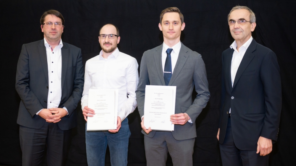
The Anton- und Klara-Röser-Stiftung awarded on the February 7th Dr. Roland Nagy with the dissertation Price. The price giving ceremony took place at the graduate celebration of the Electronics and Information Technologies department of the University of Stuttgart. The title of Dr. Roland Nagy’s thesis is „Silicon Vacancy Defects in 4H-Silicon Carbide Semiconductor for Quantum Applications “.
Nitrogen-vacancy (NV) centers in diamond are promising quantum sensors for their long spin coherence time under ambient conditions. However, their spin resonances are relatively insensitive to non-magnetic parameters such as temperature. A magnetic-nanoparticle-nanodiamond hybrid thermometer, where the temperature change is converted to the magnetic field variation near the Curie temperature, was demonstrated to have enhanced temperature sensitivity (11 mK Hz-1/2) [Phys. Rev. X 8, 011042 (2018)], but the sensitivity was limited by the large spectral broadening of ensemble spins in nanodiamonds. To overcome this limitation, we showed an improved design of a hybrid nanothermometer using a single NV center in a diamond nanopillar coupled with a single magnetic nanoparticle of copper-nickel alloy, and demonstrated a temperature sensitivity of 76 µK Hz-1/2. This hybrid design enabled detection of 2 millikelvins temperature changes with temporal resolution of 5 milliseconds. The ultra-sensitive nanothermometer offers a new tool to investigate thermal processes in nanoscale systems
References:
Ultra-sensitive hybrid diamond nanothermometer
Liu, W. Leong, K. Xia, et. al., arXiv. 1912. 12097 (2019).

Coupled micro- and nanomechanical oscillators are of fundamental and technical interest for emerging quantum technologies. Upon interfacing with long-lived solid-state spins, the coherent manipulation of the quantum hybrid system becomes possible even at ambient conditions. Although the ability of these systems to act as a quantum bus inducing long-range spin–spin interactions has been known, the possibility to coherently couple electron/nuclear spins to the common modes of multiple oscillators and map their mechanical motion to spin-polarization has not been experimentally demonstrated. We here report experiments on interfacing spins to the common modes of a coupled cantilever system and show their correlation by translating ultralow forces induced by radiation from one oscillator to a distant spin. Further, we analyze the coherent spin–spin coupling induced by the common modes and estimate the entanglement generation among distant spins.
Quantum technology relies on proper hardware, enabling coherent quantum state control as well as efficient quantum state readout. In this regard, wide-bandgap semiconductors are an emerging material platform with scalable wafer fabrication methods, hosting several promising spin-active point defects. Conventional readout protocols for defect spins rely on fluorescence detection and are limited by a low photon collection efficiency. Here, we demonstrate a photo-electrical detection technique for electron spins of silicon vacancy ensembles in the 4H polytype of silicon carbide (SiC). Further, we show coherent spin state control, proving that this electrical readout technique enables detection of coherent spin motion. Our readout works at ambient conditions, while other electrical readout approaches are often limited to low temperatures or high magnetic fields. Considering the excellent maturity of SiC electronics with the outstanding coherence properties of SiC defects, the approach presented here holds promises for scalability of future SiC quantum devices.
References
Coherent electrical readout of defect spins in silicon carbide by photo-ionization at ambient conditions; Matthias Niethammer, Matthias Widmann, Torsten Rendler, Naoya Morioka, Yu-Chen Chen, Rainer Stöhr, Jawad Ul Hassan, Shinobu Onoda, Takeshi Ohshima, Sang-Yun Lee, Amlan Mukherjee, Junichi Isoya, Nguyen Tien Son & Jörg Wrachtrup; Nature Communications volume 10, Article number: 5569 (2019), December 5th, 2019
References
M. Widmann, M. Niethammer et al., Nano Letters 2019, 19, 10, 7173-7180 September 18, 2019

A new technique inserts single-ion impurities into a crystal reliably and with a precision of tens of nanometers. Solid-state materials that contain specific impurities, such as nitrogen-vacancy centers in diamond, make promising platforms for future quantum information technologies. The quantum states of the impurities can be tailored to perform quantum logic operations, and these states can then be read out via the impurities’ fluorescence. However, implanting single-ion impurities inside crystals consistently and precisely has proved challenging. Current methods involve accelerating the ions to high energies, which allows detection of the implantation events but sacrifices spatial precision. A new implantation technique takes a step towards solving this problem. A team from Stuttgart University and Johannes Gutenberg University Mainz demonstrated that they could embed ions in a crystal at low energy to form patterns reliably and with nanometer-scale precision. The researchers insert praseodymium ions into crystals of yttrium aluminum garnet (YAG), a synthetic crystal commonly used as a lasing medium. To do this, they trap and cool praseodymium ions using lasers and electric fields. Then they accelerate the ions one at a time toward the crystal, producing an evenly spaced array 6 nm below the crystal’s surface. After annealing the crystal at 1200°C, the researchers use confocal microscopy to confirm that the impurities successfully form fluorescing color centers inside the crystal. They found that they could control the placement of the impurities to 30-nm precision and that up to 50% of the impurities fluoresced – a success rate comparable to techniques that require ion energies 3 orders of magnitude higher. In the future, the researchers say, this technique could be widely adapted to implant other types of impurities into a variety of solid-state systems.
References:
Deterministic Single-Ion Implantation of Rare-Earth Ions for Nanometer-Resolution Color-Center Generation, Karin Groot-Berning, Thomas Kornher, Georg Jacob, Felix Stopp, Samuel T. Dawkins, Roman Kolesov, Jörg Wrachtrup, Kilian Singer, and Ferdinand Schmidt-Kaler, Phys. Rev. Lett. 123, 106802 – Published 4 September 2019
References
D. D. Bhaktavatsala Rao, Sen Yang, Stefan Jesenski, Emre Tekin, Florian Kaiser, and Jörg Wrachtrup, Phys. Rev. A 100, 022307 (2019) – Published 8. August 2019
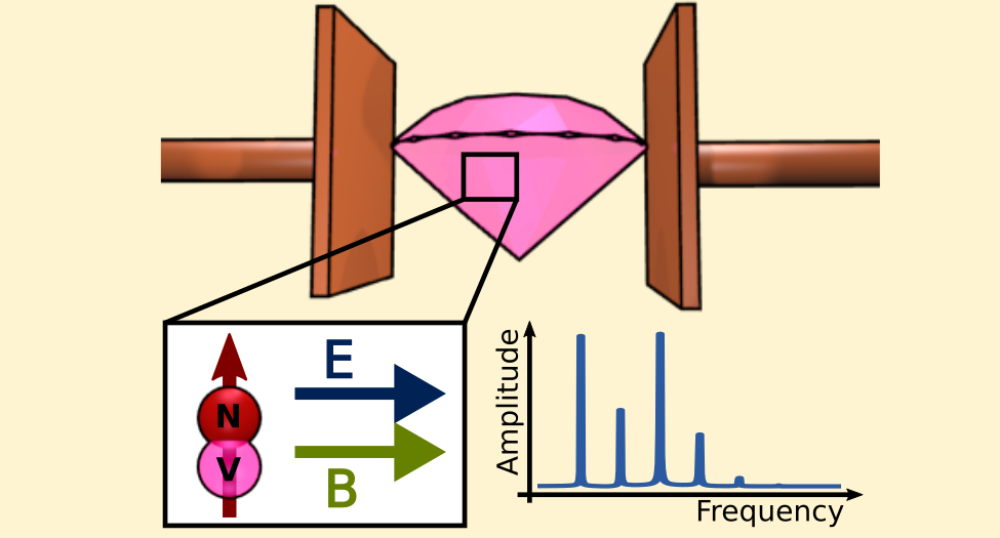
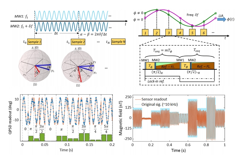
Electron spins in solids constitute formidable quantum sensors. Individual defect centers in diamond were used to detect individual nuclear spins with nanometer scale resolution, and ensemble magnetometers rival SQUID and vapor cell magnetometers when taking into account room temperature operation and size. NV center spins can also detect electric field vectors, despite their weak coupling to electric fields. Here, we employ ensembles of NV center spins to measure macroscopic ac electric vector fields with high precision. We utilize low strain, 12C enriched diamond to achieve maximum sensitivity and tailor the spin Hamiltonian via proper magnetic field adjustment to map out the ac electric field strength and polarization and arrive at refined electric field coupling constants. For high precision measurements we combine classical lock-in detection with aspects from quantum phase estimation for effective suppression of technical noise. Eventually, this enables t^-1/2 uncertainty scaling of the electric field strength over extended averaging periods, enabling us to measure electric fields down to 10^-7 V/μm for an AC electric field with a frequency of 2 kHz and an amplitude of 0.012 V/µm.
References: Robust and accurate electric field sensing with solid state spin ensembles; Nano Lett.2019, July 26, 2019, https://doi.org/10.1021/acs.nanolett.9b00900
Scalable quantum networks require stable quantum platforms with quantum processing capabilities and a reliable spin-optical interface. The search for ideal systems is still ongoing, as today’s available platforms suffer from too large electron phonon interaction and/or spectral diffusion.
The 3rd physics institute demonstrated recently that the negatively charged silicon vacancy centre in silicon carbide is immune to both drawbacks. Thanks to its 4A2 symmetry in ground and excited states, optical resonances are stable with near Fourier transform limited linewidths. In combination with millisecond long spin coherence times originating from the high purity crystal, we developed methods for high fidelity optically-assisted spin initialization and coherent control. Crucially, we showed coherent coupling to single nuclear spins with ~1 kHz resolution, which is sufficient to implement quantum memories and quantum error correction.
The summary of our findings makes the silicon vacancy in silicon carbide a prime candidate for realising memory-assisted quantum network applications using semiconductor-based spin-to-photon interfaces and coherently coupled nuclear spins.
References: Nagy et al., Nature Communications 10, 1954 (2019)
Single photon emitters in silicon carbide (SiC) are attracting attention as quantum photonic systems (Awschalom et al. Nat. Photonics 2018, 12, 516−527; Atatüre et al. Nat. Rev. Mater. 2018, 3, 38–51). However, to achieve scalable devices, it is essential to generate single photon emitters at desired locations on demand. Here we report the controlled creation of single silicon vacancy (VSi) centers in 4H-SiC using laser writing without any postannealing process. Due to the aberration correction in the writing apparatus and the nonannealing process, we generate single VSi centers with yields up to 30%, located within about 80 nm of the desired position in the transverse plane. We also investigated the photophysics of the laser writing VSi centers and concluded that there are about 16 photons involved in the laser writing VSi center process. Our results represent a powerful tool in the fabrication of single VSi centers in SiC for quantum technologies and provide further insights into laser writing defects in dielectric materials.
References:
Laser Writing of Scalable Single Color Centers in Silicon Carbide, Yu-Chen Chen, Patrick S. Salter, Matthias Niethammer, Matthias Widmann, Florian Kaiser, Roland Nagy, Naoya Morioka, Charles Babin, Jürgen Erlekampf, Patrick Berwian, Martin J. Booth, and Jörg Wrachtrup, Nano Letters, Article ASAP, 10.1021/acs.nanolett.8b05070 Publication Date (Web): March 18, 2019
Six young scientists took the over 400 spectators in the sold out Theaterhaus in ten-minutes lectures on a journey into the wondrous world of quanta. Not an easy task for the slammers. Even experts in the field describe quantum theory as incomprehensible or, like Max Born, as "hopeless mess".
Love always wins in the end. At least that's how the people in the hall saw it and chose Charles Babin, Bretone with a fresh French accent and a doctoral student at the 3rd Institute of Physics, as the winner of the evening. "Love between photons is deeper than love between people", Babin explains to us the amorous relationships between his photon friends Leon, Manon and Anton and, by the way, quantum phenomena such as entanglement, measurement and teleportation.
References: 5th Institute of Physics
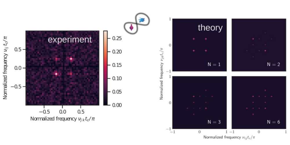
Nuclear magnetic resonance (NMR) of single spins have recently been detected by quantum sensors. However, the spectral resolution has been limited by the sensor’s relaxation to a few kHz at room temperature. This can be improved by using quantum memories, at the expense of sensitivity. In contrast, classical signals can be measured with exceptional spectral resolution by using continuous measurement techniques, without compromising sensitivity. When applied to single-spin NMR, it is critical to overcome the impact of back action inherent of quantum measurement. Here we report sequential weak measurements on a single 13C nuclear spin. The back-action causes the spin to undergo a quantum dynamics phase transition from coherent trapping to coherent oscillation. Single-spin NMR at room-temperature with a spectral resolution of 3.8 Hz is achieved. These results enable the use of measurement-correlation schemes for the detection of very weakly coupled single spins.
References
High-resolution spectroscopy of single nuclear spins via sequential weak measurements, Matthias Pfender, Ping Wang, Hitoshi Sumiya, et al., Nature Communications, Volume 10, Article number: 594 (2019)
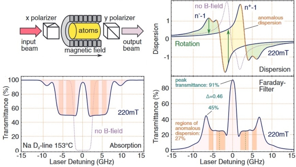
The Macaluso–Corbino effect describes the optical rotation of light in the spectral proximity to an atomic resonance. One use of this effect is narrowband optical filtering. So-called Faraday filters utilize the difference of the two components of the refractive indices, which are split by the Zeeman effect in a longitudinal magnetic field. This allows for a net rotation of a linearly polarized input beam within the medium. Placing it between crossed polarizers therefore only allows light near resonance to pass. Since any resonant spectrum implies anomalous dispersion on resonance, these filters are often characterized as being based on this anomalous dispersion. This new publication analyses to what extent the anomalous dispersion and the anomalous rotation are relevant for Faraday filters. Considering the sign of the anomalous rotation introduces a strict criterion if the filter is operated in the line center or in the spectral wing of an atomic resonance.
References
How anomalous is my Faraday filter? Optics Letters, Vol. 43, Issue 21, pp. 5295-5298 (2018), Ilja Gerhardt

Spins of impurities in solids provide a unique architecture to realize quantum technologies. A quantum register of electron and nearby nuclear spins in the lattice encompasses high-fidelity state manipulation and readout, long-lived quantum memory, and long-distance transmission of quantum states by optical transitions that coherently connect spins and photons. These features, combined with solid-state device engineering, establish impurity spins as promising resources for quantum networks, information processing and sensing. Focusing on optical methods for the access and connectivity of single spins, we review recent progress in impurity systems such as colour centres in diamond and silicon carbide, rare-earth ions in solids and donors in silicon. We project a possible path to chip-scale quantum technologies through sustained advances in nanofabrication, quantum control and materials engineering. The figure shows diverse modalities and applications of quantum sensing with impurity spins.
References
Quantum technologies with optically interfaced solid-state spins; David D. Awschalom, Ronald Hanson, Jörg Wrachtrup & Brian B. Zhou; Nature Photonics, Volume 12, pages 516–527 (2018)

References
Supported Lipid Bilayers on Fluorescent Nanodiamonds: A Structurally Defined and Versatile Coating for Bioapplications, Jan Vavra, Ivan Rehor, Torsten Rendler, Mona Jani, Jan Bednar, Michael M. Baksh, Andrea Zappe, Joerg Wrachtrup and Petr Cigler https://doi.org/10.1002/adfm.201803406
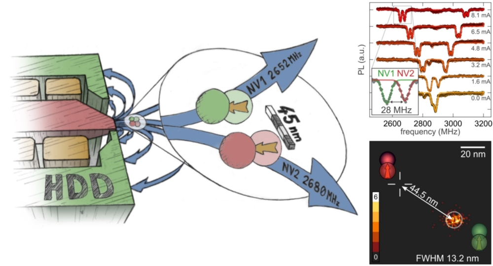
The magnetic field of a conventional hard disc drive (HDD) writer combines a high amplitude (over 200 mT) with a large gradient (up to 1 mT/nm). The usage in HDDs requires a gigahertz bandwidth that allows switching times within nanoseconds. These are much faster than characteristic timescales such as Rabi and Larmor periods, spin-spin couplings, optical transitions and spin relaxation times. The unique combination of the three features makes an HDD writer valuable for the coherent manipulation of individual spins in nanoscale networks.
In our recent experiments we exploited these properties of an HDD writer to manipulate single as well as multiple spins. With the gigahertz bandwidth we were able to drive spin transitions via non-adiabatic fast passages as well as to optically read-out the spin state in strong misaligned magnetic fields by rapidly applying control fields. Based on these techniques we used the HDD’s gradient to selectively address the spins of two parallel NVs by resonant microwave radiation with a fidelity of 99%. The individual control of the spin states allowed us to do deterministic emitter switch microscopy (DESM) to optically determine the parallel NVs’ relative distance with nanoscale resolution.
In addition, we characterized the writers’ noise level as a limiting factor for the interaction range of a coupled network. With gradients in the order of mT/nm individual spins with a few nanometer distance can be individually addressed. Therefore, HDD writers are suitable for applications in quantum information processing or sensing arrays.
Reference:
Nanoscale Spin Manipulation with Pulsed Magnetic Gradient Fields from a Hard Disc Drive Writer, Sven Bodenstedt, Ingmar Jakobi, Julia Michl, Ilja Gerhardt, Philipp Neumann, and Jörg Wrachtrup
https://dx.doi.org/10.1021/acs.nanolett.8b01387 (2018)
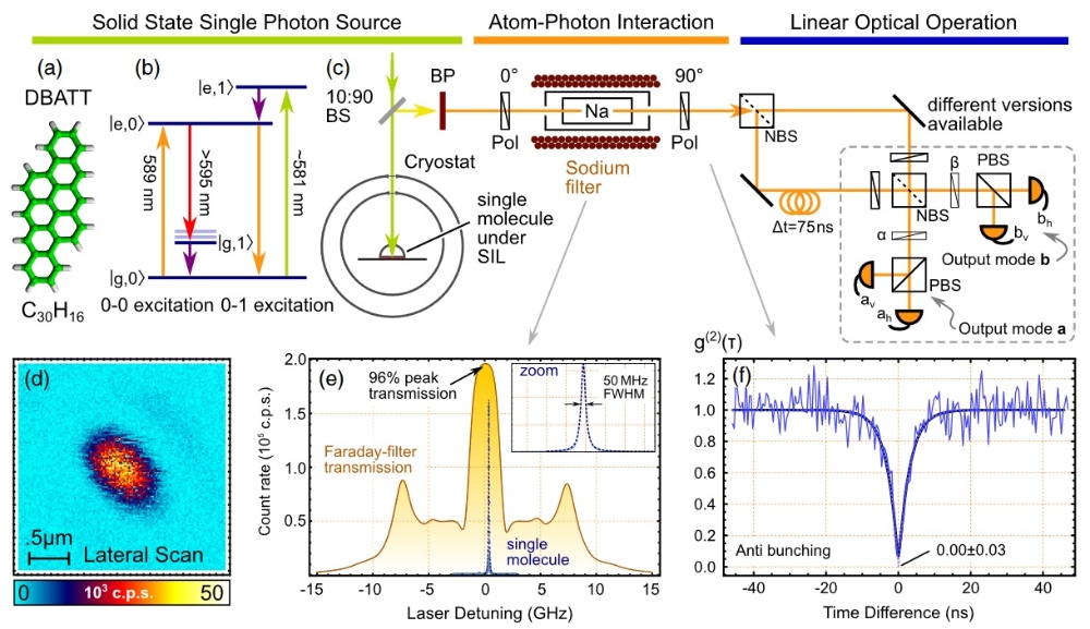
Quantum mechanics implies that a single photon can be in the superposition of two distant spatial modes and enable nonlocal interferences. The most vivid example is the two-photon coalescence on a 50∶50 beam splitter, known as Hong-Ou-Mandel interference. In the past decade, this experiment has been used to characterize the suitability of different single-photon sources for linear optical quantum gates. This characterization alone cannot guarantee the suitability of the photons in a scalable quantum network. As for a deeper insight, we perform a number of nonclassical interference measurements of single photons emitted by a single organic molecule that are optimized by an atomic Faraday filter. Our measurements reveal near unity visibility of the quantum interference, and a one-port correlation measurement proves the ideal Fourier limited nature of our single-photon source. A delayed choice quantum eraser allows us to observe a constructive interference between the photons, and a Hong-Ou-Mandel peak is formed additionally to the commonly observed dip. These experiments comprehensively characterize the involved photons for their use in a future quantum Internet, and they attest to the fully efficient interaction of the molecular photons with a next subsequent quantum node. They can be adapted to other emitters and will allow us to gain insights to their applicability for quantum information processing. We introduce a quality number that describes the photon’s properties for their use in a quantum network; this states that effectively 97% of the utilized molecular photons can be used in a scalable quantum optical system and interact with other quantum nodes. The experiments are based on a hybridization of solid state quantum optics, atomic systems, and all-optical quantum information processing.
References:
Mohammad Rezai, Jörg Wrachtrup, and Ilja Gerhardt, "Coherence Properties of Molecular Single Photons for Quantum Networks", Phys. Rev. X 8, 031026 – Published 26 July 2018
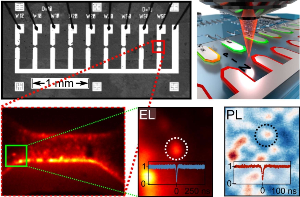
Single-photon emitting devices have been identified as an important building block for applications in quantum information and quantum communication. They allow us to transduce and collect quantum information over a long distance via photons as so-called flying qubits. In addition, substrates like silicon carbide provide an excellent material platform for electronic devices. In this work, we combine these two features and show that one can drive single photon emitters within a silicon carbide p-i-n-diode. To achieve this, we specifically designed a lateral oriented diode. We find a variety of new color centers emitting non-classical lights in the visible and near-infrared range. One type of emitter can be electrically excited, demonstrating that silicon carbide can act as an ideal platform for electrically controllable single photon sources.
References:
Matthias Widmann, Matthias Niethammer, Takahiro Makino, Torsten Rendler, Stefan Lasse, Takeshi Ohshima, Jawad Ul Hassan, Nguyen Tien Son, Sang-Yun Lee, and Jörg Wrachtrup, "Bright single photon sources in lateral silicon carbide light emitting diodes", 07 June 2018, Applied Physics Letters
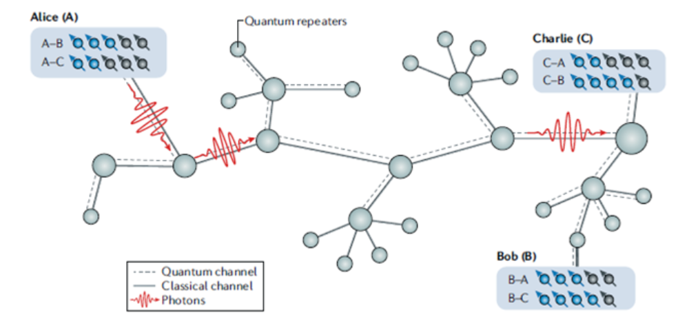
A central goal in quantum optics and quantum information science is the development of quantum networks to generate entanglement between distributed quantum memories. Experimental progress relies on the quality and efficiency of the light-matter quantum interface connecting the quantum states of photons to internal states of quantum emitters. Quantum emitters in solids, which have properties resembling those of atoms and ions, offer an opportunity for realizing light-matter quantum interfaces in scalable and compact hardware. These quantum emitters require a material platform that enables stable spin and optical properties, as well as a robust manufacturing of quantum photonic circuits. Because no emitter system is yet perfect and different applications may require different properties, several light-matter quantum interfaces are being developed in various platforms.
This Review highlights the progress in three leading material platforms: diamond, silicon carbide and atomically thin semiconductors.
References:
Material platforms for spin-based photonic quantum technologies, Mete Atatüre, Dirk Englund, Nick Vamivakas, Sang-Yun Lee and Joerg Wrachtrup, Nature Reviews Materials volume 3, pages38–51, Published: MAY 2018 , DOI: 10.1038/s41578-018-0008-9
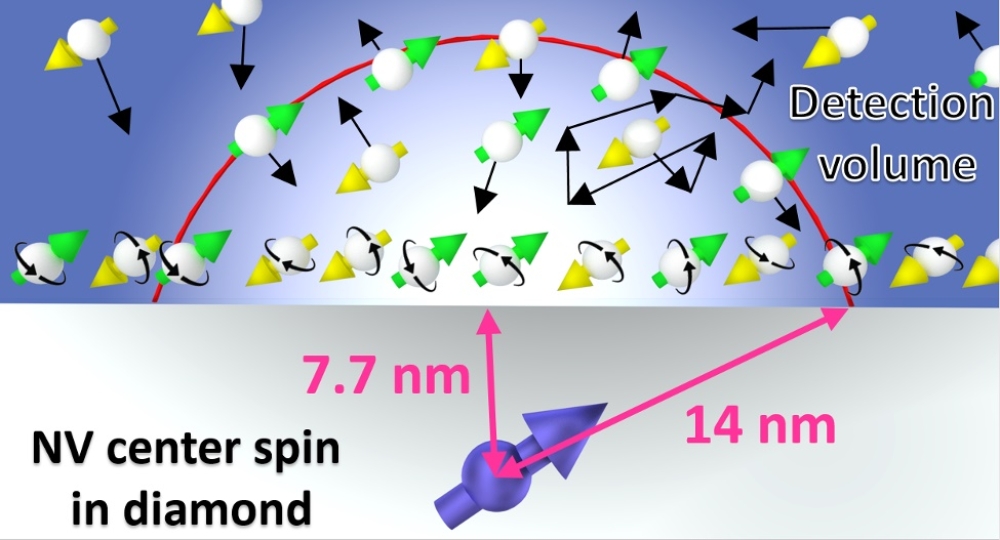
References:
F. Shagieva, S. Zaiser, P. Neumann , D. B. R. Dasari, R. Stöhr, A. Denisenko, R. Reuter, C. A. Meriles, and J. Wrachtrup, Nano Letters, Article ASAP, DOI: 10.1021/acs.nanolett.8b00925, Publication Date (Web): May 2, 2018
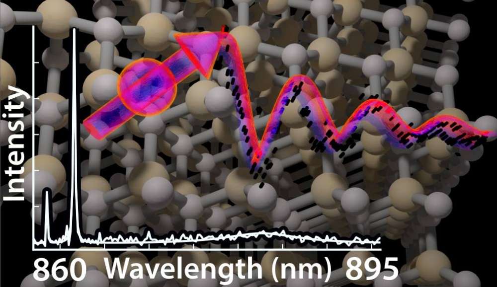
References
Quantum properties of dichroic silicon vacancies in silicon carbide, Roland Nagy, Matthias Widmann, Matthias Niethammer, Durga B. R. Dasari, Ilja Gerhardt, Öney O. Soykal, Marina Radulaski, Takeshi Ohshima, Jelena Vuckovic, Nguyen Tien Son, Ivan G. Ivanov, Sophia E. Economou, Cristian Bonato, Sang-Yun Lee, and Jörg Wrachtrup, Phys. Rev. Applied, 2018
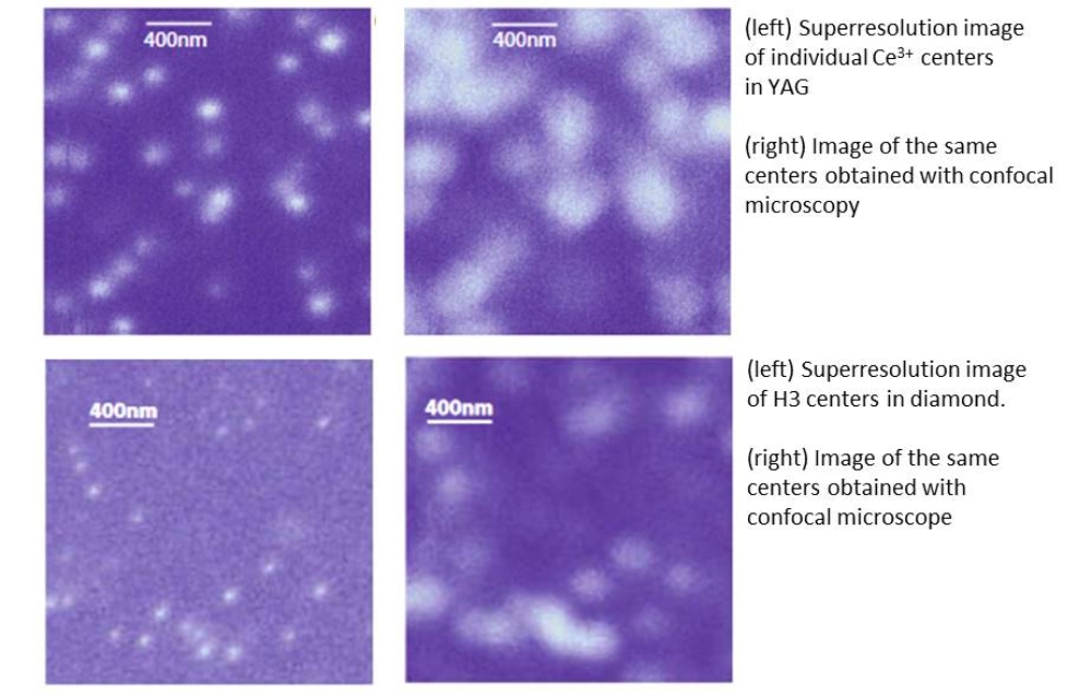
References:
Superresolution Microscopy of Single Rare-Earth Emitters in YAG and H3 Centers in Diamond, R. Kolesov, S. Lasse, C. Rothfuchs, A.D. Wieck, K. Xia, T. Kornher, and J. Wrachtrup, Phys. Rev. Lett. 120, 033903 – Published 19 January 2018
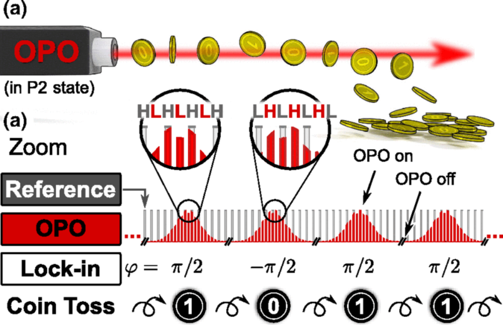
References:
Unbiased All-Optical Random-Number Generator, Tobias Steinle, Johannes N. Greiner, Jörg Wrachtrup, Harald Giessen, and Ilja Gerhardt, Phys. Rev. X 7, 041050 – Published 30 November 2017
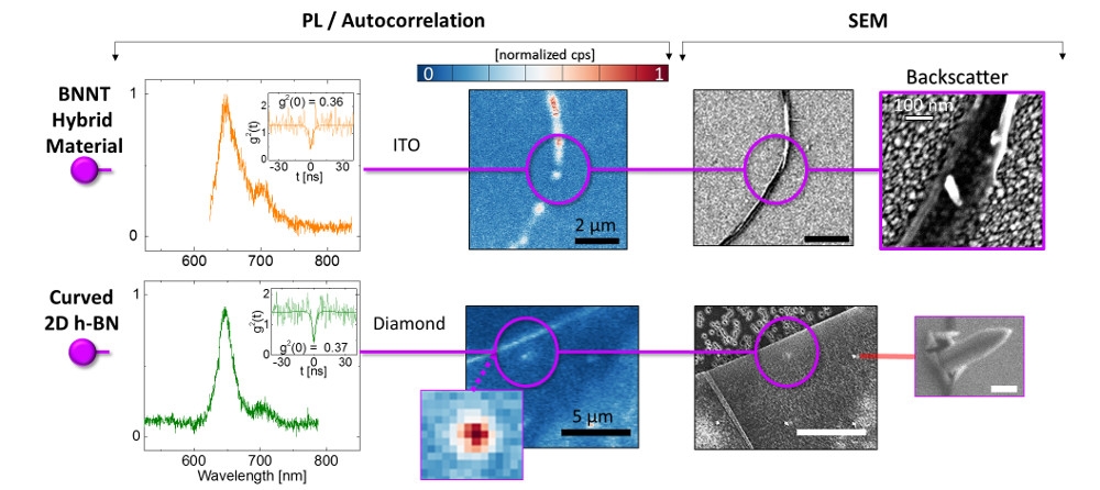
References:
Quantum Light in Curved Low Dimensional Hexagonal Boron Nitride Systems, Nathan Chejanovsky, Youngwook Kim, Andrea Zappe, Benjamin Stuhlhofer, Takashi Taniguchi, Kenji Watanabe, Durga Dasari, Amit Finkler, Jurgen H. Smet & Jörg Wrachtrup, Scientific Reports 7, Article number: 14758 (2017) doi:10.1038/s41598-017-15398-2
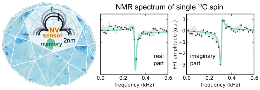
The key components of our sensing device are a single electron spin quantum sensor and a non-volatile nuclear spin quantum memory. We avoid back action and retain sensor performance by temporarily storing classical information about samples on the memory and by dynamically decoupling the sensor from both memory and sample. With our novel device design and observation methods, we identify sample spins with spectral discrimination down to 13 Hz.
Our results improve the characterization of small spin clusters. For example, we pave the way for chemical structure analysis on nanoscopic volumes via nuclear magnetic resonance spectroscopy techniques, which are typically applied to millimeter scale samples.
References:
Nonvolatile nuclear spin memory enables sensor-unlimited nanoscale spectroscopy of small spin clusters, M. Pfender, N. Aslam, H. Sumiya, S. Onoda, P. Neumann, J. Isoya, C. A. Meriles & J. Wrachtrup, Nature Communications 8, 834 (2017).
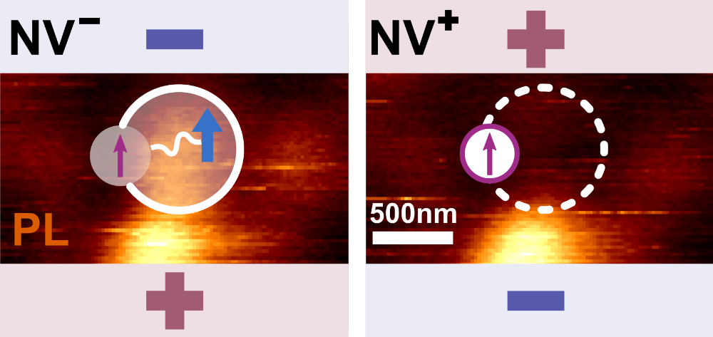
Switching on and off the coupling of proximal nuclear spins to the outside world
In recent years, solid-state spin systems have emerged as promising candidates for quantum information processing and sensing applications. Prominent examples are the nitrogen-vacancy (NV) center in diamond, phosphorous dopants in silicon (Si:P), rare-earth ions in solids and V Si -centers in silicon-carbide. Typically, nuclear spins serve as memories whereas the electron spins of these candidate systems grant access to the memories in the first place. For example, the NV center electron spin state determines the photoluminescence response. In all these systems, however, the electron spin is not only a gift but also a burden. Its fast relaxation decreases the quantum memory’s lifetime. The Si:P system has demonstrated that its nuclear spins can yield exceedingly long quantum memory lifetimes by eliminating the electron spin of the dopant. For NV centers, however, a proper charge state for storage of quantum information has not been identified yet. In our recent publication, we have identified and characterized the positively-charged NV center as an electron-spin-less and optically inactive state by utilizing the nuclear spin qubit as a probe. We have controlled the electronic charge and spin utilizing nanometer scale gate electrodes. As a result, we have improved the quantum memory’s lifetime by a factor of four. Surprisingly, the new charge state allows switching the optical response of single NV spin systems facilitating full individual addressability even in dense arrays with mutual distances below the optical diffraction limit. Our results, open up new and promising possibilities for scaling up magnetic-dipole-coupled, NV center quantum registers in diamond. Furthermore, improved quantum storage times and optical switching improve applications in quantum communication, as for example in quantum repeaters.
Figure: Two photoluminescence (PL) microscopy images of the same NV center in different charge states (NV -, NV +). The polarity (+,-) of adjacent electrodes allows setting the charge state. While NV - exhibits an electron and a nuclear spin (blue and purple arrow), NV +only possesses a nuclear spin, which is therefore very isolated from many noise sources.
References:
M. Pfender, N. Aslam, P. Simon, D. Antonov, G. Thiering, S. Burk, F. Fávaro de Oliveira, A. Denisenko, H. Fedder, J. Meijer, J. A. Garrido, A. Gali, T. Teraji, J. Isoya, M. W. Doherty, A. Alkauskas, A. Gallo, A. Grüneis, P. Neumann, and J. Wrachtrup, Protecting a diamond quantum memory by charge state control, Nano Lett. (2017), doi: 10.1021/acs.nanolett.7b01796
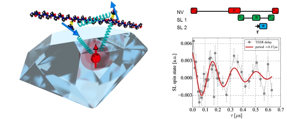
Applications of quantum technologies will require an unprecedented level of complexity and control of the system at the nanoscale, while retaining precision and scalability in the fabrication. The identification and characterization of suitable elementary building blocks for such technologies is crucial.
Here we present such a basic unit, a synthetic polypeptide chain with electronic spin bearing side groups. These so called spin labels are attached at specific sites of the molecular backbone using chemistry methods and separated at almost arbitrary distances, here a few nanometers. The molecular spins are controlled and read out using a nitrogen vacancy (NV) center in diamond, which provides pure optical access of single quantum states. We demonstrate the feasibility of coherent spin manipulation and access of the direct dipolar coupling tensor of pairs of S=1/2 electronic spins close to the single molecular level (? 3 doubly labeled molecules). The pairwise dipolar coupling of spins is found to be ~5.5 ± 1 MHz, in agreement with the designed intra-molecular spin-spin distance. These results show for the first time, that arbitrary molecular quantum spin networks can be accessed on the single molecular level, thus opening the path to applications like molecular quantum simulators, quantum information processing, or single molecular structure determination.
References:
Molecular quantum spin network controlled by a single qubit, Lukas Schlipf, Thomas Oeckinghaus, Kebiao Xu, Durga Bhaktavatsala Rao Dasari, Andrea Zappe, Felipe Fávaro de Oliveira, Bastian Kern, Mykhailo Azarkh, Malte Drescher, Markus Ternes, Klaus Kern, Jörg Wrachtrup, Amit Finkler, Science Advances 2017
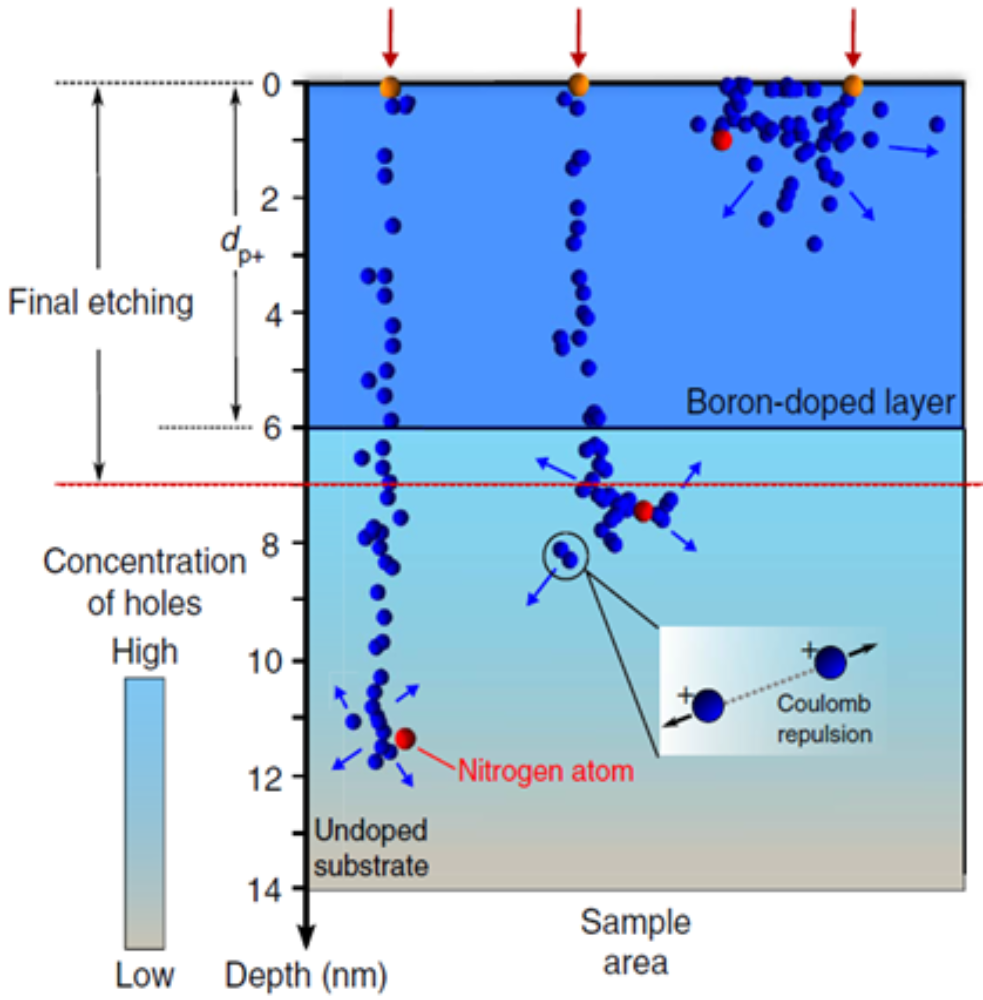
Atomic-size spin defects in solids are unique quantum systems. Most applications require nanometer positioning accuracy, which is typically achieved by low-energy ion implantation. A drawback of this technique is the significant residual lattice damage, which degrades the performance of spins in quantum applications. Here we show that the charge state of implantation-induced defects drastically influences the formation of lattice damage during implantation and thermal annealing. Charging of vacancies at, for example, nitrogen implantation sites suppresses the formation of vacancy complexes, resulting in tenfold-improved spin coherence times and twofold-improved formation yield of nitrogen-vacancy centers in diamond. This is achieved by confining implantation defects into the space-charge layer of free carriers (holes) generated within a p + -i junction structures with overgrown layer of diamond with high concentration of boron acceptors. Combined with numerical calculations, these results bring new insights into the dynamic mechanisms of self-diffusion and defect formation at single implantation sites. In the future, the concept of defect charging could be implemented into various solid-state systems for improved engineering of quantum devices.
References:
F. F. de Oliveira, et al. Nat. Commun. 8, 15409 doi: 10.1038/ncomms15409 (2017)
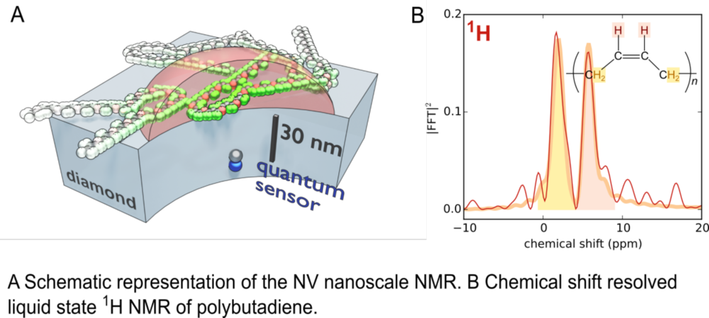
Nuclear magnetic resonance (NMR) is a valuable technique that has found application in hospitals in the form of magnetic resonance imaging (MRI). Furthermore NMR spectroscopy has been used in laboratories to identify almost all known molecules. The main limiting factor is its low sensitivity requiring millimeter-sized samples. This has been overcome by using the nitrogen-vacancy (NV) center in diamond as a NMR probe and decreased the required sample volume by many orders of magnitude down to the nanometer-scale [1]. Previous NV nanoscale NMR studies however showed poor spectral resolution making it unfeasible for spectroscopy. In our recent NV nanoscale NMR work [2], we demonstrate an improvement of the spectral resolution by a factor of 10,000 and resolve chemical shift effects in proton and fluorine containing molecules.
These results were enabled by multiple factors: The NV sensor was combined with the nitrogen nuclear spin serving as a quantum memory in order to increase the relaxation time of the whole NMR probe to more than four minutes. Next, a magnetic field of 3 Tesla was applied to distinguish between different chemical shift groups within a molecule. Furthermore the sample sensor interaction time was increased by adjusting the detection volume. Finally, applying homonuclear decoupling sequences also allowed high resolution nanoscale NMR of solid samples.
[1] Nuclear Magnetic Resonance Spectroscopy on a (5-Nanometer)³ Sample Volume, T. Staudacher, F. Shi, S. Pezzagna, J. Meijer, J. Du, C. A. Meriles, F. Reinhard & J. Wrachtrup, Science 339, 561 (2013).
[2] Nanoscale nuclear magnetic resonance with chemical resolution, N. Aslam, M. Pfender, P. Neumann, R. Reuter, A. Zappe, F. Fávaro de Oliveira, A. Denisenko, H. Sumiya, S. Onoda, J. Isoya, J. Wrachtrup, Science 357, 67 (2017).
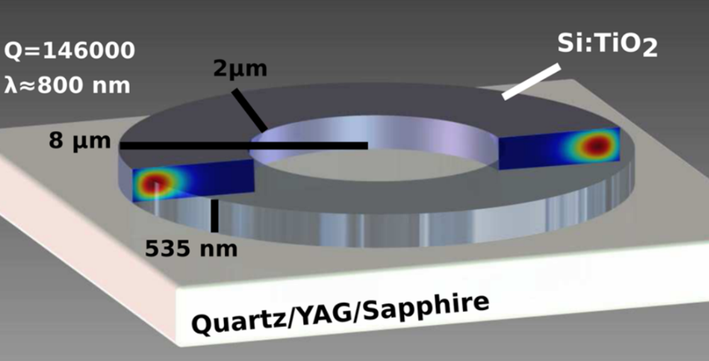
High quality optical thin film materials form a basis for on-chip photonic micro- and nanodevices, where several photonic elements form an optical circuit. Their realization generally requires the thin film to have a higher refractive index than the substrate material. Here, we demonstrate a method of depositing amorphous TiO 2 films doped with 25% Si on various substrates, a way of shaping these films into photonic elements, such as optical waveguides and resonators, and finally, the performance of these elements.
The quality of the film is estimated by measuring thin film cavity Q-factors in excess of 10 5 at a wavelength of 790 nm, corresponding to low propagation losses of 5.1dB/cm. With a refractive index of n > 2, the film supports waveguiding on different substrates, such as quartz, YAG, and sapphire, and shows evanescent coupling to chromium ions embedded in YAG, presenting film-substrate interaction. Additional functionalization of the films by doping with optically active rare-earth ions such as erbium is also demonstrated. Thus, Si:TiO 2 films allow for creation of high quality photonic elements, both passive and active, and also provide access to a broad range of substrates and emitters embedded therein.
Reference:
T. Kornher, K. Xia, R. Kolesov, B. Villa, S. Lasse, et al., Amorphous Silicon-Doped Titania Films for on-Chip Photonics, ACS Photonics, Publication Date (Web): April 13, 2017, DOI: 10.1021/acsphotonics.6b00919
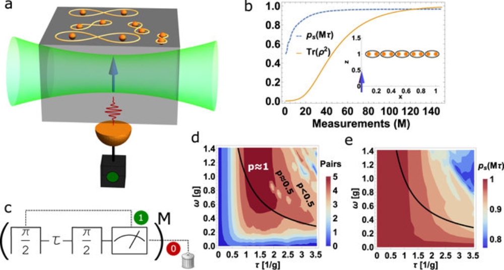
Dynamical polarization of nuclear spin ensembles is of central importance for magnetic resonance studies, precision sensing and for applications in quantum information theory. Here we propose a scheme to generate long-lived singlet pairs in an unpolarized nuclear spin ensemble which is dipolar coupled to the electron spins of a Nitrogen Vacancy center in diamond. The quantum mechanical back-action induced by frequent spin-selective readout of the NV centers allows the nuclear spins to pair up into maximally entangled singlet pairs. Counterintuitively, the robustness of the pair formation to dephasing noise improves with increasing size of the spin ensemble. We also show how the paired nuclear spin state allows for enhanced sensing capabilities of NV centers in diamond.
References
Purification of an unpolarized spin ensemble into entangled singlet pairs
Johannes N. Greiner, Durga Bhaktavatsala Rao Dasari & Jörg Wrachtrup
Scientific Reports 7, Article number: 529 (2017), doi:10.1038/s41598-017-00603-z
Dissipative entanglement of solid-state spins in diamond
Generating robust entanglement among solid-state spins is key for applications in quantum information processing and precision sensing. Here we show a dissipative approach to generate such entanglement among the hyperfine coupled electron nuclear spins using the rapid optical decay of electronic excited states. The combined dark state interference effects of the optical and microwave driving fields in the presence of spontaneous emission from the short-lived excited state leads to a dissipative formation of an entangled steady state. We show that the dissipative entanglement is generated for any initial state conditions of the spins and is resilient to external field fluctuations. We analyze the scheme for both continuous and pulsed driving fields in the presence of realistic noise sources.
References
Dissipative entanglement of solid-state spins in diamond
Durga Bhaktavatsala Rao Dasari, Sen Yang & Jörg Wrachtrup
PHYSICAL REVIEW A, 95, 022310 (2017) DOI:10.1103/PhysRevA.95.022310
Silicon carbide is a promising platform for single photon sources [1], quantum bits (qubits), and nanoscale sensors [2] based on individual color centers. Toward this goal, we develop a scalable array of nanopillars incorporating single silicon vacancy centers in 4H-SiC, readily available for efficient interfacing with free-space objective and lensed-fibers.
A commercially obtained substrate is irradiated with 2 MeV electron beams to create vacancies. Subsequent lithographic process forms 800 nm tall nanopillars with 400–1400 nm diameters. We obtain high collection efficiency of up to 22 kcounts/s optical saturation rates from a single silicon vacancy center while preserving the single photon emission and the optically induced electron-spin polarization properties. Our study demonstrates silicon carbide as a readily available platform for scalable quantum photonics architecture relying on single photon sources and qubits. The joint work of the international team of researchers in the US, Germany, Korea, Sweden and Japan have published the work in Nano Letters [3].
References
[1] M. Widmann, S.-Y. Lee, T. Rendler, et al., Coherent control of single spins in silicon carbide at ambient condition , Nat. Mater.
(2015) 1–21.
[2] M. Niethammer, M. Widmann, S.-Y. Lee, P. Stenberg, O. Kordina, T.
Ohshima, et al., Vector Magnetometry Using Silicon Vacancies in 4H-SiC Under Ambient Conditions, Phys. Rev. Appl. 6 (2016)
[3] M. Radulaski & M. Widmann, M. Niethammer, J.L. Zhang, S.-Y. Lee, T.
Rendler, et al., Scalable Quantum Photonics with Single Color Centers in Silicon Carbide, Nano Lett. 17 (2017) 2–6.
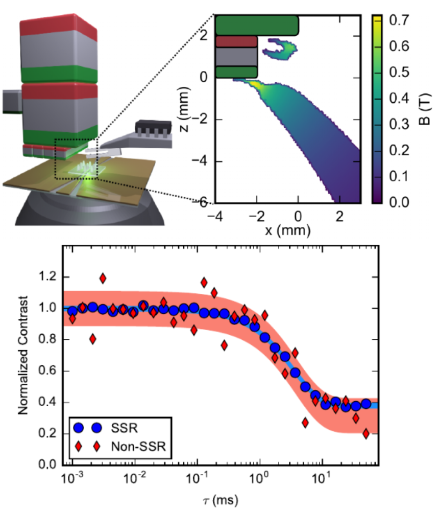
Magnetic sensing and imaging instruments are important tools in biological and material sciences. There is an increasing demand for attaining higher sensitivity and spatial resolution, with implementations using a single qubit offering potential improvements in both directions. In this article we describe a scanning magnetometer based on the nitrogen-vacancy center in diamond as the sensor. By means of a quantum-assisted readout scheme together with advances in photon collection efficiency, our device exhibits an enhancement in signal to noise ratio of close to an order of magnitude compared to the standard fluorescence readout of the nitrogen-vacancy center. This is demonstrated by comparing non-assisted and assisted methods in a T1 relaxation time measurement.
Reference:
Nuclear quantum-assisted magnetometer
Review of Scientific Instruments, Volume 88, Issue 1, 10.1063/1.4973449
Thomas Häberle, Thomas Oeckinghaus, Dominik Schmid-Lorch, Matthias Pfender, Felipe Fávaro de Oliveira, Seyed Ali Momenzadeh, Amit Finkler and Jörg Wrachtrup

Newly discovered van der Waals materials like MoS2, WSe2, hexagonal boron nitride (h-BN) and recently C2N have sparked intensive research to unveil the quantum behavior associated with their 2D structure. Of great interest are 2D materials that host single quantum emitters. h-BN, with a band-gap of –5.95 eV, has been shown to host single quantum emitters which are stable at room temperature in the UV and visible spectral range. Here we investigate correlations between h-BN structural features and emitter location from bulk down to the mono-layer at room temperature. We demonstrate that chemical etching and ion irradiation can generate emitters in h-BN. We analyze the emitters’ spectral features and show that they are dominated by the interaction of their electronic transition with a single Raman active mode of h-BN. Photo-dynamics analysis reveals diverse rates between the electronic states of the emitter. The emitters show excellent photo stability even under ambient conditions and in monolayers. Comparing the excitation polarization between different emitters unveils a connection between defect orientation and the h-BN hexagonal structure. The sharp spectral features, color diversity, room-temperature stability, long lived meta-stable states, ease of fabrication, proximity of the emitters to the environment, outstanding chemical stability and biocompatibility of h-BN provide a completely new class of systems that can be used for sensing and quantum photonics applications.
Reference
Structural Attributes and Photodynamics of Visible Spectrum Quantum Emitters in Hexagonal Boron Nitride
Nathan Chejanovsky, Mohammad Rezai, Federico Paolucci, Youngwook Kim, Torsten Rendler, Wafa Rouabeh, Felipe Fávaro de Oliveira, Patrick Herlinger, Andrej Denisenko, Sen Yang, Ilja Gerhardt, Amit Finkler, Jurgen H. Smet and Jörg Wrachtrup
Link (extern): http://pubs.acs.org/doi/abs/10.1021/acs.nanolett.6b03268

A joint research team of the University of Stuttgart and the Max Planck institute for solid state research has recently performed an experiment which combines the state-of-the-art research on quantum dots and atomic vapors. The work, led by the scientists Ilja Gerhardt (3rd Institute of Physics, University of Stuttgart and MPI) and Simone Luca Portalupi (Institute of semiconductor optics and functional interfaces – IHFG, University of Stuttgart), aims to integrate the ideal properties of solid-state based single photon sources, which are spectrally aligned to an atomic transition.
The quantum dot single-photon source is specially selected from an in-house grown sample to match exactly the resonance of atomic cesium vapor. Under strong coherent resonant excitation, the emission is split into a so-called Mollow-triplet, which emits light distributed on three distinct spectral lines. The optical emission emits the photons one by one, unlike a light bulb or e.g. the sun. These non-classical single photon sources can be extremely narrow-band and extremely bright, and open the opportunity for quantum communication and quantum information protocols.
A fundamental requirement for interfacing different, distant sources is currently challenging due to different linewidth and color of the solid-state-based single photon sources. The current work aims to face this challenge, producing photons which are precisely set in energy, meaning that they can be effectively used in the realization of quantum repeaters.
As a matter of fact the atomic vapor is also used as the primary time standard in industry. Here it is used as a Faraday filter to precisely select specific lines from the quantum dots, which are emitting bright and high quality single photons. The atoms act as a special frequency reference and extremely narrow-band filter. Their exact color, in scientific terms their spectral linewidth, is many thousand times narrower than e.g. some normal colored dye.
The presented research is along the line of quantum hybrid systems, and aims to integrate the work usually performed by different research teams: the vision being the integration of solid-state quantum optics and atomic spectroscopy onto a unified platform. In future such research will enable novel quantum technologies, such as secure remote communications and precision measurements, which utilize the quantum properties of nature to enhance sensitivity and set new precision standards.
The work was recently published in Nature Communications:
Nature Communications 7, 13632 (2016), doi:10.1038/ncomms13632

In a collaboration with Seagate Technology PLC, we have developed methods to characterize the magnetic fields of hard-disk writers using an atomic scale magnetometer. The results mark a significant increase in spatial resolution compared to established sensors and may enable further miniaturization of recording heads and ultimately increase storage capacities of hard disk drives (HDD).
HDDs store data as permanent magnetization on sectors as small as 20 nm on the recording medium of the hard disk. In order to encode data as magnetization bits the hard disk writer, a nanoscopic electromagnet, has to produce magnetic fields that only affect a single bit while it flies by on the rotating disk. Accordingly, its magnetic field is designed to be strong, fast and especially local. These features are beyond the capabilities of established magnetometers leaving the industry devoid of a suitable research and development tool to further miniaturize their products.
We deployed the nitrogen-vacancy defect center in diamond (NV) as magnetometer to resolve this challenging magnetic field. By scanning the HDD writer of the surface of a diamond we could record its magnetic field optically using a single shallow NV. As the NV is an atomic size point defect our spatial resolution only depends on the positioning of the writer.
Besides introducing quantum metrology to manufacturers of mass consumer products, the work also shows that HDD writers may be a viable control tool for NV related research where its unique features, namely its exceptional field strength (1T), gradient (10 mT/nm) and bandwidth (GHz), enable new experiments in spintronics, quantum information processing and magnetic resonance imaging on the nanoscale.
Reference:
Measuring broadband magnetic fields on the nanoscale using a hybrid quantum register
Ingmar Jakobi, Philipp Neumann, Ya Wang, Durga Bhaktavatsala Rao Dasari, Fadi El Hallak, Muhammad Asif Bashir, Matthew Markham, Andrew Edmonds, Daniel Twitchen and Jörg Wrachtrup
http://dx.doi.org/10.1038/nnano.2016.163
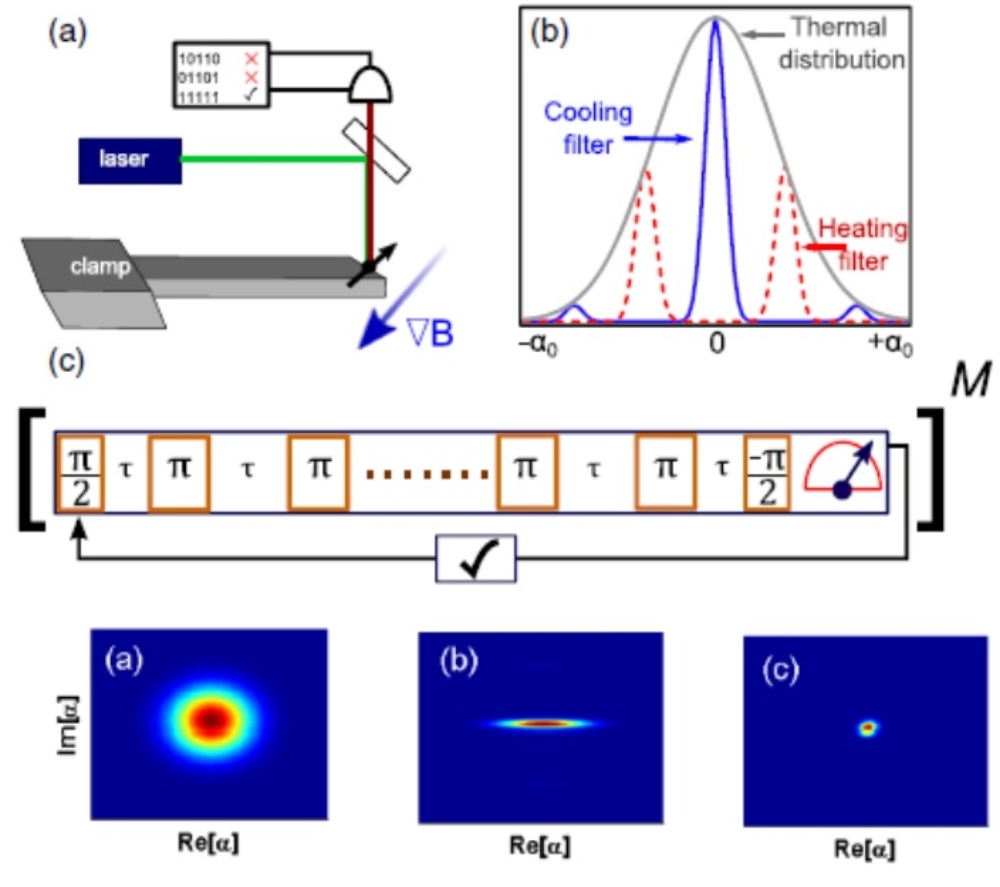
Heralded Control of Mechanical Motion by Single Spins
We propose a method to achieve a high degree of control of nanomechanical oscillators by coupling their mechanical motion to single spins. Manipulating the spin alone and measuring its quantum state heralds the cooling or squeezing of the oscillator even for weak spin-oscillator couplings. We analytically show that the asymptotic behavior of the oscillator is determined by a spin-induced thermal filter function whose overlap with the initial thermal distribution of the oscillator determines its cooling, heating, or squeezing. Counterintuitively, the rate of cooling dependence on the instantaneous thermal occupancy of the oscillator renders robust cooling or squeezing even for high initial temperatures and damping rates. We further estimate how the proposed scheme can be used to control the motion of a thin diamond cantilever by coupling it to its defect centers at low temperature.
Thin Circular Diamond Membrane with Embedded Nitrogen-Vacancy Centers for Hybrid Spin-Mechanical Quantum Systems
Coupling mechanical degrees of freedom to single well-controlled quantum systems has become subject to intense research recently. Here, we report on the design, fabrication, and characterization of a diamond architecture consisting of a high-quality thin circular diamond membrane with embedded near-surface nitrogen-vacancy centers (NVCs). To demonstrate this architecture, we employ the NVCs by means of their optical and spin interfaces as nanosensors of the motion of the membrane under static pressure and in-resonance vibration. We also monitor the static residual stress within the membrane using the same method. Driving the membrane at its fundamental resonance mode, we observe coupling of this vibrational mode to the spin of the NVCs. Our realization of this architecture can manifest the applications of diamond structures in 3D piezometry such as mechanobiology and vibrometry, as well as mechanically mediated spin-spin coupling in quantum-information science.
References:
Heralded Control of Mechanical Motion by Single Spins
D.D. Bhaktavatsala Rao, S. Ali Momenzadeh, and Jörg Wrachtrup
Phys. Rev. Lett. 117, 077203 – Published 11 August 2016
http://dx.doi.org/10.1103/PhysRevLett.117.077203
Thin Circular Diamond Membrane with Embedded Nitrogen-Vacancy Centers for Hybrid Spin-Mechanical Quantum Systems
S. Ali Momenzadeh, Felipe Fávaro de Oliveira, Philipp Neumann, D.D. Bhaktavatsala Rao, Andrej Denisenko, Morteza Amjadi, Zhiqin Chu, Sen Yang, Neil B. Manson, Marcus W. Doherty, and Jörg Wrachtrup
Phys. Rev. Applied 6, 024026 – Published 31 August 2016
http://dx.doi.org/10.1103/PhysRevApplied.6.024026

Different approaches have improved the sensitivity of either electron or nuclear magnetic resonance to the single spin level. For optical detection it has essentially become routine to observe a single electron spin or nuclear spin. Typically, the systems in use are carefully designed to allow for single spin detection and manipulation, and of those systems, diamond spin defects rank very high, being so robust that they can be addressed, read out and coherently controlled even under ambient conditions and in a versatile set of nanostructures. This renders them as a new type of sensor, which has been shown to detect single electron and nuclear spins among other quantities like force, pressure and temperature. Adapting pulse sequences from classic NMR and EPR, and combined with high resolution optical microscopy, proximity to the target sample and nanoscale size, the diamond sensors have the potential to constitute a new class of magnetic resonance detectors with single spin sensitivity. As diamond sensors can be operated under ambient conditions, they offer potential application across a multitude of disciplines. Here we review the different existing techniques for magnetic resonance, with a focus on diamond defect spin sensors, showing their potential as versatile sensors for ultra-sensitive magnetic resonance with nanoscale spatial resolution.
Reference: Journal of Magnetic Resonance, Volume 269, August 2016, Pages 225–236, Perspectives in Magnetic Resonance – Single spin magnetic resonance, Jörg Wrachtrup and Amit Finkler
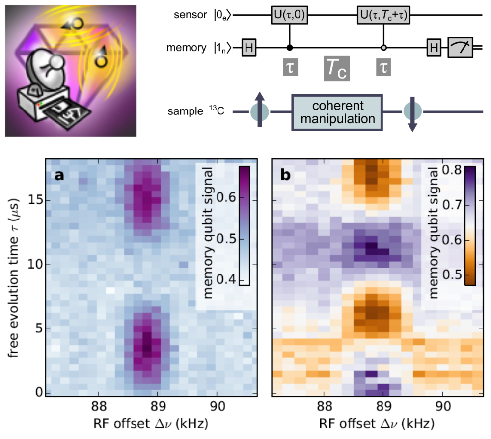
In quantum sensing, precision is typically limited by the maximum time interval over which phase can be accumulated. Memories have been used to enhance this time interval beyond the coherence lifetime and thus gain precision. Here, we demonstrate that by using a quantum memory also an increased sensitivity can be achieved. To this end, we use entanglement in a hybrid spin system comprising a sensing and a memory qubit associated with a single nitrogen-vacancy center in diamond (see upper figure part). With the memory we retain the full quantum state even after coherence decay of the sensor, which enables coherent interaction with distinct weakly coupled nuclear spin qubits (see lower figure part). To this end we do tomography of the memory’s quantum phase as we increase the interaction time τ with a sample qubit (here: 13C spin, a: cos φ, b: sin φ ). The phase is only accumulated when the sample spin is resonantly driven during the storage time T c. The spectral selectivity is determined by 1/T c which is much narrower than what is possible with the sensor alone. Furthermore, we benchmark the performance of our hybrid quantum system against use of the sensing qubit alone by gradually increasing the entanglement of sensor and memory. Finally, we further apply this quantum sensor-memory pair for high-resolution NMR spectroscopy of single 13C nuclear spins.
The results of our work are published in:
S. Zaiser, T. Rendler, I. Jakobi, T. Wolf, S.-Y. Lee, S. Wagner, V. Bergholm, T. Schulte-Herbrüggen, P. Neumann, and J. Wrachtrup, Enhancing quantum sensing sensitivity by a quantum memory. Nature Communications 7, 12279 (2016).
A tool for accurate and quantitative extraction of resonant vibrational responses
A novel approach based on the wavelet prism decomposition analysis is proposed to correct experimental artefacts in a coherent anti-Stokes Raman scattering (CARS) spectrum. In collaboration with Erik Vartiainen and co-workers of the Lappeenranta University in Finland, Gregor Hehl and Andreas Volkmer demonstrate that this method allows estimating and eliminating a slowly varying modulation error function in the measured normalized CARS spectrum and yields a corrected CARS line-shape. The main advantage of the approach is that any corrections of the spectral phase and amplitude are avoided in the retrieved vibrational line-shape spectrum, thus significantly simplifying the quantitative reconstruction of the sample’s Raman response from a normalized CARS spectrum in the presence of experimental artefacts. Moreover, unlike in conventional error-correction schemes, the method obviates the need for assumptions about the modulation error distribution and the chemical composition of the specimens under study. The method is quantitatively validated on normalized CARS spectra recorded for equimolar aqueous solutions of D-fructose, D-glucose, and their disaccharide combination sucrose. Besides being essential for the realization of quantitative multiplex CARS imaging applications, this method also offers a tool for accurate and quantitative reconstruction of complex material responses probed by other nonlinear optical spectroscopies, such as for the correction of experimental errors in measured third-harmonic generation, sum-frequency generation, and degenerate four-wave mixing power spectra.
Reference:
Y. Kan, L. Lensu, G. Hehl, A. Volkmer*, and E.M. Vartiainen*, Opt. Express 24 (2016) 11905-11916.
Link (extern): doi: 10.1364/OE.24.011905
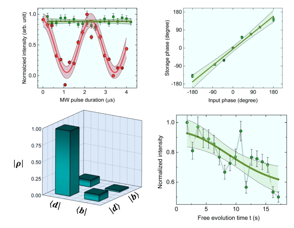
Long distance quantum communication requires photons and quantum nodes that comprise qubits for interaction with light, good memory capabilities and processing qubits for storage and manipulation of photons. Owing to the unavoidable photon losses, robust quantum communication over lossy transmission channels requires quantum repeater networks. A necessary and highly demanding requirement for these networks is the existence of quantum memories with long coherence times to reliably store the incident photon states. Here, we demonstrate a high fidelity (~98%) coherent transfer of a photon polarisation state to a single solid state nuclear spin that has a coherence time of over 10 seconds. The storage process is achieved by coherently transferring the polarisation state of a photon to an entangled electron-nuclear spin state of a nitrogen vacancy (NV) centre in diamond. This nuclear spin based optical quantum memory demonstrated here paves the way towards an absorption based quantum repeater network.
Reference:
Nature Photonics | Letter
High-fidelity transfer and storage of photon states in a single nuclear spin
Sen Yang, Ya Wang, D. D. Bhaktavatsala Rao, Thai Hien Tran, Ali S. Momenzadeh, M. Markham, D. J. Twitchen, Ping Wang, Wen Yang, Rainer Stöhr, Philipp Neumann, Hideo Kosaka & Jörg Wrachtrup
Nature Photonics (2016) doi:10.1038/nphoton.2016.103 Published online: 06 June 2016
PhD Student Kangwei Xia Receives Prestigious 2015 Chinese Government Award for Outstanding Self-Financed Students Abroad
The award is set-up to honor overseas non-Chinese-government funded Chinese PhD students with outstanding academic accomplishments across all disciplines. This year, 35 PhD students studying in Germany received this award. Kangwei Xia is the 12th.award winner studying at University of Stuttgart since 2003. The prize amount for this award is $6,000, sponsored by the Chinese Ministry of Education.
Kangwei Xia is a 4th year PhD student in our institute. His research topic is spectroscopy of single rare earth solid-state qubits, including optical detection, coherent manipulation and optical readout different species single rare earth ions in crystals.
Link (external): 2015 Chinese Government Award for Extra-Outstanding Self-Financed Students
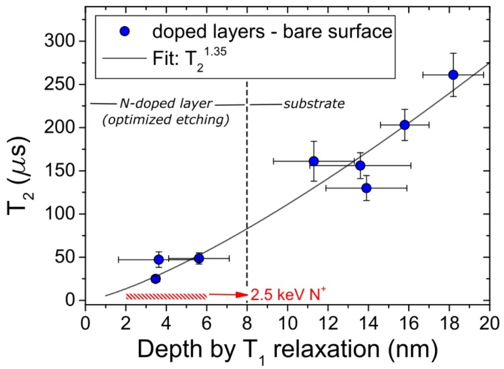
Toward Optimized Surface δ – Profiles of Nitrogen-Vacancy Centers Activated by Helium Irradiation in Diamond
The negatively-charged nitrogen-vacancy (NV) center in diamond has been shown recently as an excellent sensor for external spins. Nevertheless, their optimum engineering in the near-surface region still requires quantitative knowledge in regard to their activation by vacancy capture during thermal annealing. To this aim, we report on the depth profiles of near-surface helium-induced NV centers (and related helium defects) by step-etching with nanometer resolution. This provides insights into the efficiency of vacancy diffusion and recombination paths concurrent to the formation of NV centers. It was found that the range of efficient formation of NV centers is limited only to approximately 10 to 15nm (radius) around the initial ion track of irradiating helium atoms. Using this information we demonstrate the fabrication of nanometric-thin (δ) profiles of NV centers for sensing external spins at the diamond surface based on a three-step approach, which comprises (i) nitrogen-doped epitaxial CVD diamond overgrowth, (ii) activation of NV centers by low-energy helium irradiation and thermal annealing, and (iii) controlled layer thinning by low-damage plasma etching. Spin coherence times (Hahn echo) ranging up to 50 μs are demonstrated at depths of less than 5nm in material with 1.1% of 13 C (depth estimated by spin relaxation (T 1) measurements). At the end, the limits of the helium irradiation technique at high ion fluences are also experimentally investigated.
Reference:
Nano Letters, 2016, 16 (4), pp 2228–2233
Felipe Fávaro de Oliveira, S. Ali Momenzadeh, Denis Antonov, Jochen Scharpf, Christian Osterkamp, Boris Naydenov, Fedor Jelezko, Andrej Denisenko, and Jörg Wrachtrup
DOI: 10.1021/acs.nanolett.5b04511
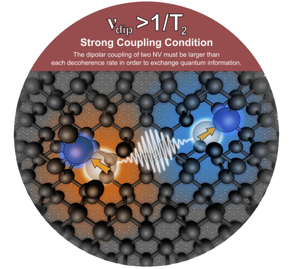
Coherently coupled pairs or multimers of nitrogen-vacancy defect centers (NV) in diamond have many promising applications especially in quantum information processing. Scalable registers are essential to the progress of the field. Ion implantation is the only technique known to produce NV pairs close enough to be coupled with dipolar interaction. However, while there are many approaches to increase the resolution of ion implantation, no method is able to reliably produce working registers. Together with the density of implanted nitrogen the density of unwanted defects (e.g. divacancies) related to the implantation is also increased, resulting in inferior qubits. Here we present an estimation what nanomask implantation parameters (energy, fluence and aperture size) are most likely to produce interacting qubits. We apply our findings to an easily reproducible implantation technique, the e-beam lithography in PMMA, to create coupled NV pairs with a reasonable probability.
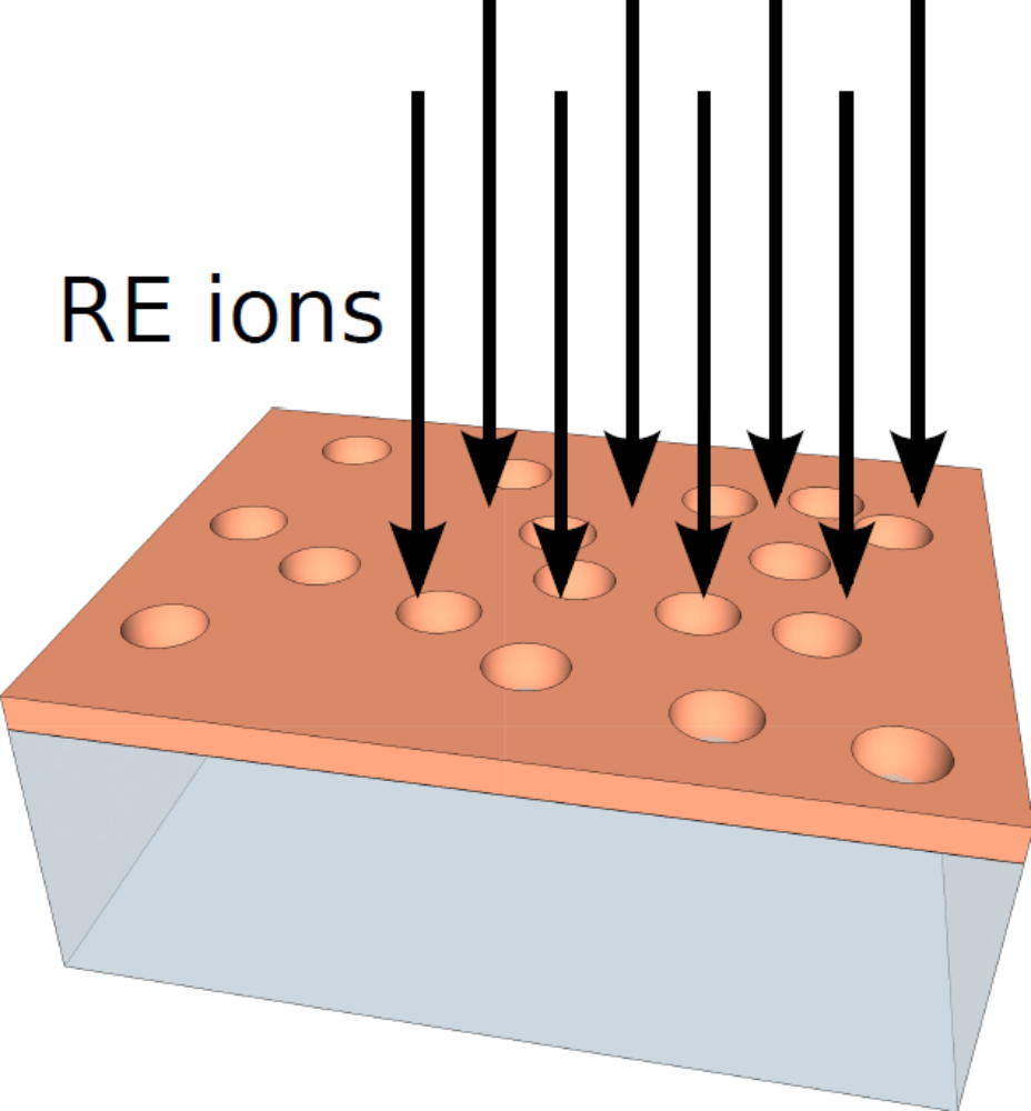
Appl. Phys. Lett. 108, 053108 (2016); http://dx.doi.org/10.1063/1.4941403
Rare-earth (RE) ion doped crystals are well known due to their key application in laser technology. Latest research, however, suggests their usage in the field of quantum telecommunication as quantum memories or even for information processing. Their generation in a well chosen and engineered environment can act as a prerequisite for versatile implementation of RE ions in experiments and might enable a range of novel integrated photonic devices for quantum applications.
Controlled doping into desired locations of optical crystals was achieved by ion implantation. We have investigated the production yield of two RE species, namely cerium and praseodymium. As a measure, the collected fluorescence intensity from both implanted samples and single centers was used. With a tailored annealing procedure for cerium, a yield up to 53% was estimated. Praseodymium yield amounts up to 91%. Such high implantation yield indicates a feasibility of creation of nanopatterned rare-earth doping and suggests strong potential of RE species for on-chip photonic devices.

Erneute hochrangige Auszeichnung für Jörg Wrachtrup, 04.01.16
Für seine herausragenden Arbeiten zur Quantentechnologie erhält Prof. Jörg Wrachtrup, Leiter des 3. Physikalischen Instituts, den ZEISS Research Award 2016. Er wird gemeinsam mit seinem ehemaligen Kollegen Prof. Fedor Jelezko (Universität Ulm) für die Forschung über die Wechselwirkung von Licht mit Elektronenspins in Diamant ausgezeichnet.
Ein renommierter Preis für renommierte Forschung
Der ZEISS Research Award wird alle zwei Jahre vergeben. Dotiert ist er mit einem Preisgeld von 40.000 Euro. Die Kandidaten haben bereits herausragende Leistungen im Bereich der Optik oder Photonik demonstriert. Ihre Arbeiten besitzen ein hohes Potential für weitere Erkenntnisse und praktische Anwendungen. Die aktuelle Ehrung findet im Rahmen des ZEISS Symposiums am 23. Juni 2016 in Oberkochen statt.
Weiter zum vollständigen Artikel
© Foto (Jelezko): Elvira Eberhardt
© Foto (Wrachtrup): David Ausserhofer
The application of masers is limited by its demanding working conditions (high vacuum or low temperature). A room-temperature solid-state maser is highly desirable, but the lifetimes of emitters (electron spins) in solids at room temperature are usually too short (~ns) for population inversion. Masing from pentacene spins in p-terphenyl crystals, which have a long spin lifetime (~0.1 ms), has been demonstrated. This maser, however, operates only in the pulsed mode. Here we propose a room-temperature maser based on nitrogen-vacancy centres in diamond, which features the longest known solid-state spin lifetime (~5 ms) at room temperature, high optical pumping efficiency (~10 6 Hz) and material stability. Our numerical simulation demonstrates that a maser with a coherence time of approximately minutes is feasible under readily accessible conditions (cavity Q-factor ~5×10 4, diamond size ~3×3×0.5mm³ and pump power <10 W). A room-temperature diamond maser may facilitate a broad range of microwave technologies.
Reference: Proposal for a room-temperature diamond maser
Liang Jin, Matthias Pfender, Nabeel Aslam, Philipp Neumann, Sen Yang, Jörg Wrachtrup & Ren-Bao Liu, Nature Communications 6, Article number: 8251, doi:10.1038/ncomms9251, Published 23 September 2015
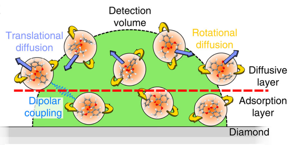
via an individual paramagnetic centre
We demonstrate a protocol using individual nitrogen-vacancy centres in diamond to observe the time evolution of proton spins from organic molecules located a few nanometres from the diamond surface. The protocol records temporal correlations among the interacting protons, and thus is sensitive to the local dynamics via its impact on the nuclear spin relaxation and interaction with the nitrogen vacancy. We gather information on the nanoscale rotational and translational diffusion dynamics by analysing the time dependence of the nuclear magnetic resonance signal. Applying this technique to liquid and solid samples, we find evidence that liquid samples form a semi-solid layer of 1.5-nm thickness on the surface of diamond, where translational diffusion is suppressed while rotational diffusion remains present. Extensions of the present technique could be exploited to highlight the chemical composition of molecules tethered to the diamond surface or to investigate thermally or chemically activated dynamical processes such as molecular folding.
Picture: We assume a layered model in the detection volume (green semi-sphere) comprising a static adsorption film (red dashed line) where translational diffusion (light blue arrows, rotational diffusion as yellow arrows) of the molecules (orange spheres) is prohibited, and a mobile, outer section in which molecules self-diffuse as in a bulk liquid.
Reference: Probing molecular dynamics at the nanoscale via an individual paramagnetic centre, T. Staudacher, N. Raatz, S. Pezzagna, J. Meijer, F. Reinhard, C. A. Meriles & J. Wrachtrup, Nature Communications 6, Article number: 8527, doi:10.1038/ncomms9527, Published 12 October 2015
... on shallow nitrogen-vacancy centers in diamond
Near-surface nitrogen-vacancy (NV) centers in diamond have been successfully employed as atomic-sized magnetic field sensors for external spins over the last years. A key challenge is still to develop a method to bring NV centers at nanometer proximity to the diamond surface while preserving their optical and spin properties. To that aim we present a method of controlled diamond etching with nanometric precision using an oxygen inductively coupled plasma process. Importantly, no traces of plasma-induced damages to the etched surface could be detected by X-ray photoelectron spectroscopy and confocal photoluminescence microscopy techniques. In addition, by profiling the depth of NV centers created by 5.0 keV of nitrogen implantation energy, no plasma-induced quenching in their fluorescence could be observed. Moreover, the developed etching process allowed even the channeling tail in their depth distribution to be resolved. Furthermore, treating a 12 C isotopically purified diamond revealed a threefold increase in T 2 times for NV centers with <4 nm of depth (measured by nuclear magnetic resonance signal from protons at the diamond surface) in comparison to the initial oxygen-terminated surface.
Reference: Effect of low-damage inductively coupled plasma on shallow nitrogen-vacancy centers in diamond, Felipe Fávaro de Oliveira, S. Ali Momenzadeh, Ya Wang, Mitsuharu Konuma, Matthew Markham, Andrew M. Edmonds, Andrej Denisenko and Jörg Wrachtrup, Appl. Phys. Lett. 107, 073107 (2015); Link (extern): http://dx.doi.org/10.1063/1.4929356
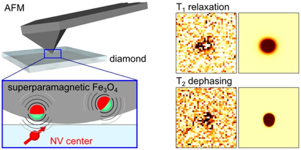
of Superparamagnetic Magnetite Nanoparticles Using a Single Qubit
To study the magnetic dynamics of superparamagnetic nanoparticles, we use scanning probe relaxometry and dephasing of the nitrogen vacancy (NV) center in diamond, characterizing the spin noise of a single 10 nm magnetite particle. Additionally, we show the anisotropy of the NV sensitivity’s dependence on the applied decoherence measurement method. By comparing the change in relaxation (T1) and dephasing (T2) time in the NV center when scanning a nanoparticle over it, we are able to extract the nanoparticle’s diameter and distance from the NV center using an Ornstein–Uhlenbeck model for the nanoparticle’s fluctuations. This scanning probe technique can be used in the future to characterize different spin label substitutes for both medical applications and basic magnetic nanoparticle behavior.
Reference: Relaxometry and Dephasing Imaging of Superparamagnetic Magnetite Nanoparticles Using a Single Qubit, Dominik Schmid-Lorch, Thomas Häberle, Friedemann Reinhard, Andrea Zappe, Michael Slota, Lapo Bogani, Amit Finkler, and Jörg Wrachtrup, Nano Lett., Article ASAP, DOI: 10.1021/acs.nanolett.5b00679, Publication Date (Web): July 28, 2015
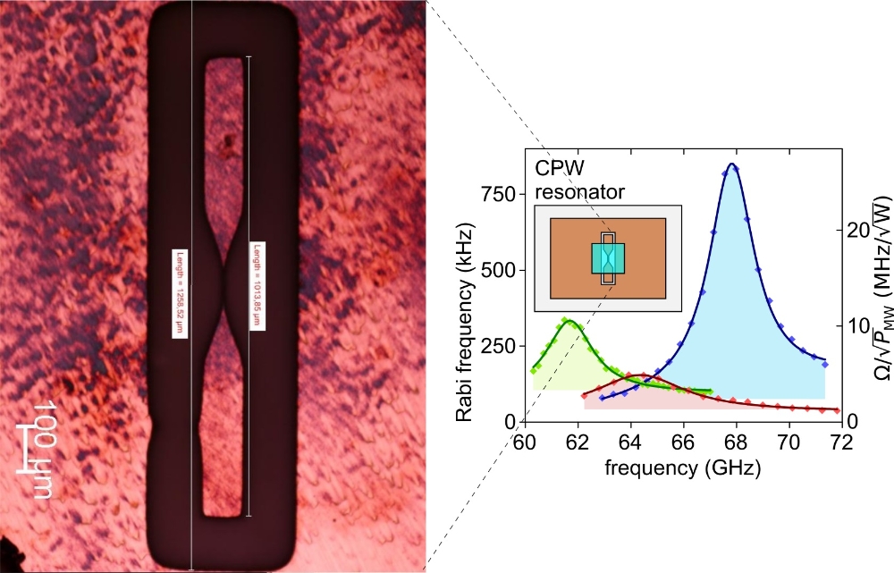
Single electron and nuclear spin magnetic resonance experiments in the context of quantum information processing and nanoscale metrology can benefit strongly from high magnetic fields.
The product basis of e.g. an electron and a nuclear spin becomes closer and closer to the eigenenergy basis. In addition, when it comes to sensing and distinguishing single molecules, the chemical shift is a handy fingerprint, and the latter gets larger and therefore better detectable for higher magnetic fields. So far single electron spin experiments were performed at magnetic fields up to 1.6 T (Si:P). Here, we explore the frequency range up to 90 GHz, respectively magnetic fields of up to 3T for single spin magnetic resonance in conjunction with optical spin readout. To exploit the available low power amplifiers in the corresponding E-band fullest, we develop suitable microwave resonators. We demonstrate the benefit of higher magnetic fields by showing longer nuclear spin lifetimes than in previous studies.
Reference: Single spin optically detected magnetic resonance with 60–90 GHz (E-band) microwave resonators
Nabeel Aslam, Matthias Pfender, Rainer Stöhr, Philipp Neumann, Marc Scheffler, Hitoshi Sumiya, Hiroshi Abe, Shinobu Onoda, Takeshi Ohshima, Junichi Isoya, and Jörg Wrachtrup
Review of Scientific Instruments, 86, 064704 (2015); doi: 10.1063/1.4922664
View online: http://dx.doi.org/10.1063/1.4922664
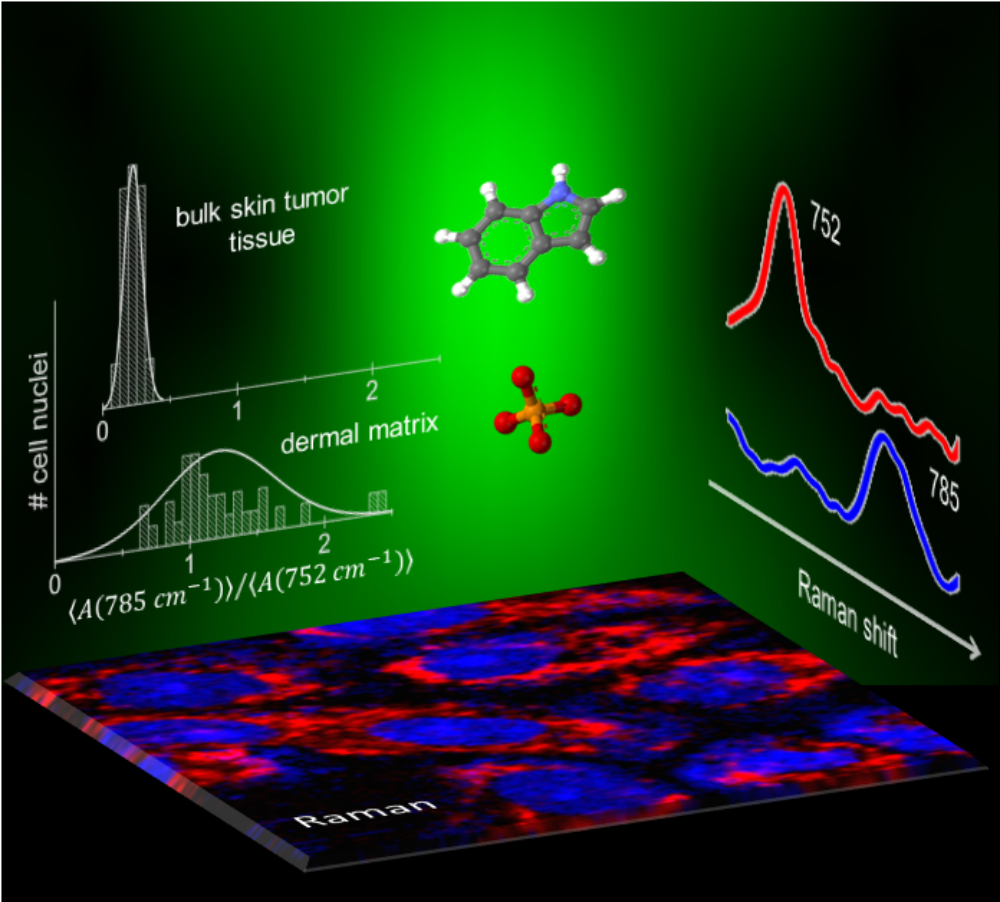
... of Nucleic Acids and Tryptophan for Distinction of Normal Human Skin Cells and Tumorigenic Keratinocytes
Tumor diagnostic imaging is commonly based on staining of biopsies, which requires tissue excision, fixation, and staining with exogenous marker molecules. Here, P. Piredda and A. Volkmer demonstrate label-free tumor imaging using confocal spontaneous Raman scattering microspectroscopy, which exploits the intrinsic vibrational contrast of endogenous biomolecular species. In a collaboration with M. Berning and P. Boukamp of the DKFZ in Heidelberg, we present a chemically specific and quantitative approach to monitoring normal human skin cells as well as the human HaCaT in vitro skin carcinogenesis model and the tumor-derived MET in vivo skin cancer progression model. Mapping the amplitudes of two spectrally well isolated Raman bands allowed for direct visualization of the distributions representative of tryptophan-rich proteins and nucleic acids with subcellular spatial resolution. Using these Raman markers, it was feasible to discriminate between normal human epidermal keratinocytes and dermal fibroblasts, and to confine all tumorigenic cells from both. First evidence for the successful application of the proposed intracellular nucleic acid and tryptophan Raman signatures for skin cancer diagnosis was further demonstrated in an organotypic cutaneous squamous cell carcinomas model, allowing for the identification of tumor cells and their surrounding stroma in the tissue context.
Reference: P. Piredda, M. Berning, P. Boukamp, and A. Volkmer, Subcellular Raman Microspectroscopy Imaging of Nucleic Acids and Tryptophan for Distinction of Normal Human Skin Cells and Tumorigenic Keratinocytes, Anal. Chem. 87 (2015), advance online, DOI: 10.1021/acs.analchem.5b01009
Link (extern): Publication
Universität Stuttgart, 6. März 2015. Diamant-Sensor macht einzelne Proteine in natürlicher Umgebung sichtbar
Proteine sind die zentralen Bausteine des Lebens. Zellen beispielsweise sind aus einer Vielzahl verschiedener Proteinen zusammengesetzt. Ihr Zusammenspiel bestimmt praktisch alle wichtigen biologischen Funktionen und entscheidet über Gesundheit beziehungsweise Krankheit von Organismen. Proteine selbst bestehen aus vielen Tausend Atomen, deren genaue Anordnung die Funktionsweise des Proteins bestimmt. Entsprechend begehrt sind Verfahren, die es erlauben, die genaue Form und Dynamik von Proteinen in ihrer natürlichen Umgebung zu untersuchen. Ein internationales Forscherteam der Universität Stuttgart und der Chinesischen Akademie der Wissenschaften ist dabei nun einen entscheidenden Schritt vorangekommen. Darüber berichtet die Zeitschrift Science in Ihrer Ausgabe vom 6. März 2015.
Der Gruppe um Prof. Jörg Wrachtrup vom 3. Physikalischen Institut der Universität Stuttgart und Prof. Jiangfeng Du ist es gelungen, mit einem neuen Verfahren einzelne Proteine in natürlicher Umgebung sichtbar zu machen. Dazu haben sie einen neuen Sensor benutzt, der auf einzelnen Defekten in Diamant beruht. Die Defekte können Magnetfelder in ihrer Umgebung nachweisen und sind zum Beispiel empfindlich genug, um das Feld einzelner Elektronen detektieren zu können. Dies haben die Forscher ausgenutzt, um die Proteine sichtbar zu machen.
Originalpublikation:
Single-protein Spin Resonance Spectroscopy under Ambient Conditions
Fazhan Shi,Qi Zhang, Pengfei Wang, Hongbin Sun, Jiarong Wang, Xing Rong, Ming Chen, Chenyong Ju, Friedemann Reinhard, Hongwei Chen, Jörg Wrachtrup, Junfeng Wang, Jiangfeng Du
Link (extern): http://www.sciencemag.org/content/347/6226/1135
Paola Cappellaro, Professor at MIT is elected Mercator-Fellow of the recently funded DFG Research Group “Diamond Materials for Quantum Application”. Prof. Cappellaro is an internationally known expert in quantum spin physics with major contributions to NMR and diamond spin physics. In particular she focussed on the analysis of diamond-based nano magnetometry. Recently, she concentrated on applications to nuclear spin polarisation in combination with NMR structure analysis of single proteins. The Mercator-Fellowship endows the mutual research project and cooperation among Prof. Cappellaro and members of the research group. (Photo: Research Laboratory of Electronics)
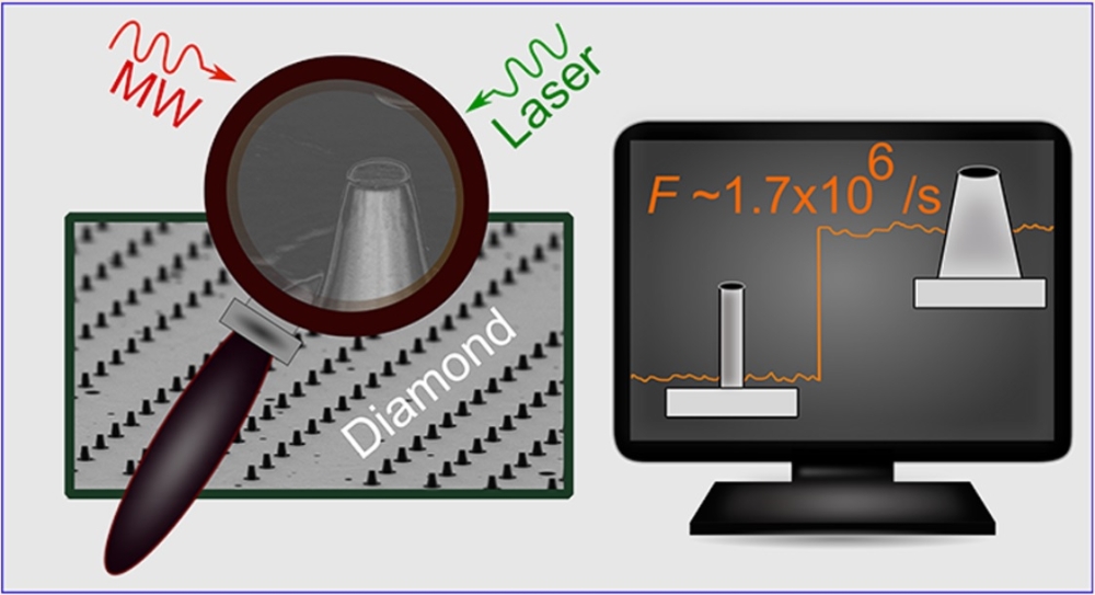
Nanoengineered Diamond Waveguide as a Robust Bright Platform for Nanomagnetometry Using Shallow Nitrogen Vacancy Centers
Photonic structures in diamond are key to most of its application in quantum technology. Here, we demonstrate tapered nanowaveguides structured directly onto the diamond substrate hosting shallow-implanted nitrogen vacancy (NV) centers. By optimization based on simulations and precise experimental control of the geometry of these pillar-shaped anowaveguides, we achieve a net photon flux up to ~ 1.7 × 10 6 s -1. This presents the brightest monolithic bulk diamond structure based on single NV centers so far. We observe no impact on excited state lifetime and electronic spin dephasing time (T 2) due to the nanofabrication process. Possessing such high brightness with low background in addition to preserved spin quality, this geometry can improve the current nanomagnetometry sensitivity ~ 5 times. In addition, it facilitates a wide range of diamond defects-based magnetometry applications. As a demonstration, we measure the temperature dependency of T 1 relaxation time of a single shallow NV center electronic spin. We observe the two-phonon Raman process to be negligible in comparison to the dominant two-phonon Orbach process.
Figure 2. A SEM image of an array of tapered nanopillars (scale bar = 3 µm). B SEM image of a diamond tapered nanopillar; height ~ 1.2 µm, top diameter ~ 400 nm, and bottom diameter ~ 900 nm (scale bar = 500 nm). C Confocal image of the tapered nanopillars (2.5 keV energy of implantation) under ambient conditions (scale bar = 5 µm).
Reference: dx.doi.org/10.1021/nl503326t | NanoLett. 2015, 15, 165-169
Author(s): S. Ali Momenzadeh, Rainer J. Stöhr, Felipe Favaro de Oliveira, Andreas Brunner, Andrej Denisenko, Sen Yang, Friedemann Reinhard, and Jörg Wrachtrup
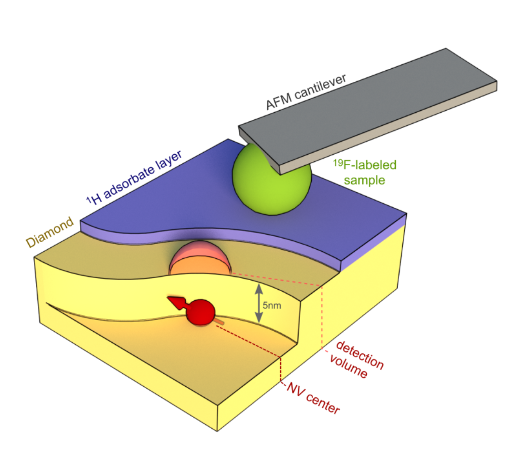
with chemical contrast by nanoscale nuclear magnetic resonance
Scanning probe microscopy is one of the most versatile windows into the nanoworld, providing imaging access to a variety of electronic, dielectric, magnetic and topographic sample properties. We demonstrate a scanning probe imaging method that extends the range of accessible quantities to label-free imaging of chemical species while operating on arbitrary samples – including insulating materials – under ambient conditions. Moreover, its sensitivity extends below the surface of a sample, allowing for imaging of subsurface features. We achieve these results by recording NMR signals from a sample surface with a recently introduced scanning probe, a single nitrogen-vacancy centre in diamond. We demonstrate NMR imaging with 10 nm resolution and achieve chemically specific contrast by separating fluorine from hydrogen-rich regions. Our result opens the door to scanning probe imaging of the chemical composition and molecular structure of arbitrary samples.
Reference: Häberle, T., Schmid-Lorch, D., Reinhard, F. & Wrachtrup, J. Nanoscale nuclear magnetic imaging with chemical contrast. Nat. Nanotechnol. advance on, (2015), DOI: 10.1038/nnano.2014.299.
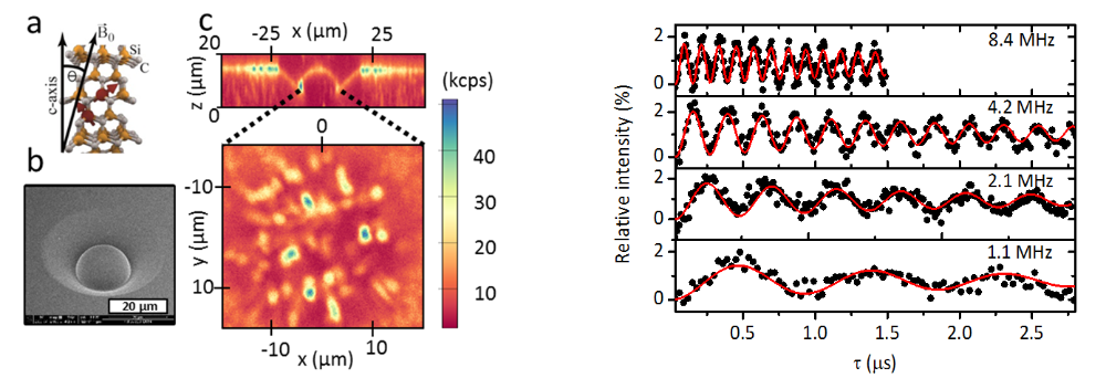
Spins in solids are cornerstone elements of quantum spintronics. Leading contenders such as defects in diamond or individual phosphorus dopants in silicon have shown spectacular progress, but either lack established nanotechnology or an efficient spin/photon interface. Silicon carbide (SiC) combines the strength of both systems: it has a large bandgap with deep defects and benefits from mature fabrication techniques. We report the characterization of photoluminescence and optical spin polarization from single silicon vacancies in SiC, and demonstrate that single spins can be addressed at room temperature. We also show coherent control of a single defect spin and find long spin coherence times under ambient conditions. Our study provides evidence that SiC is a promising system for atomic-scale spintronics and quantum technology.
Left: a, 4H–SiC crystal structure and spins at silicon vacancies. b, Scanning electron microscope image of the fabricated solid immersion lens (SIL) on the surface. c, Confocal fluorescence image scanned around the fabricated hemispherical SIL with laser excitation at 730 nm showing defects (bright spots) inside the SIL. Right: Spin Rabi oscillations of a single silicon vacancy ground state.
Reference:
Matthias Widmann et al., Coherent control of single spins in silicon carbide at room temperature. Nature Materials (2014) doi:10.1038/nmat4145
Featured in a News and Views by Andrea Morello in Nature Materials; Quantum spintronics: Single spins in silicon carbide.

When specialized devices are not commercially available, they have to be developed in house – and that pays off. This was realized recently also by two groups of students and post docs from the 3rd Physics Institute, who went ahead and commercialized their electronics developments.
Markus Wick, Marco Di Sarno and Helmut Fedder developed an 8 channel streaming time-to-digital converter with ~20 ps resolution in FPGA fabric that is now sold by the newly founded company 'Swabian Instruments'. “The key feature of the device is the versatile software backend that allows an unlimited number of data analysis threads to hook onto the time tag stream in real time”, say the developers.
LK-Instruments, founded by Kim Kafenda and Stefan Lasse, developed an new generation of rotary stages for precise positioning of optical research-equipment. They beard the lack of table-top and manual controllable positioning devices by providing an easy to use and full-featured computer interface at the same time for all computer platforms.
With these new developed tools and their new concepts of usage, research at the 3rd Physics Institute got much faster, more precise and more comfortable for all our researchers.
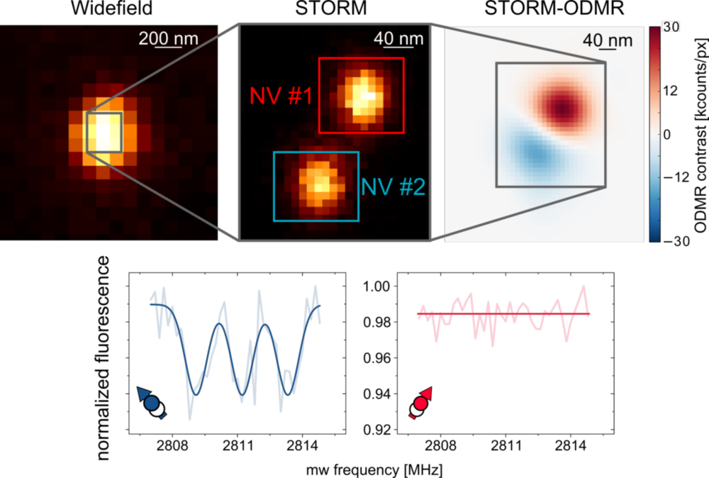
Mastering nanoscopic quantum systems promises applications in quantum information processing (QIP) and nanoscale metrology. However, the spatial density of individually addressable systems is not only limited by their size, but rather by the scale needed for control and readout. This affects upscaling of QIP devices and limits nanoscale sensors to be scanning probe devices with serial data acquisition. Here, we simultaneously apply parallel nanoscale microscopy and spin resonance methods on ensembles of optically addressable spins. The latter have been applied as qubits and nanoscale quantum sensors on the single level. In contrast, our method allows parallel individual addressing inside ensembles of qubits/sensors with nanometer distances. This promises a vast speedup for sensing applications compared with scanning probe methods.
Reference:
Single-spin stochastic optical reconstruction microscopy
PNAS, September 5, 2014, Matthias Pfender, et.al., doi: 10.1073/pnas.1404907111

The DFG research group FOR 1493 “Diamond Materials and Quantum Applications” goes into its second funding period.
FOR1493 is a national research consortium funded by the Deutsche Forschungs-gemeinschaft. The strategic aim of the research group is to foster quantum material science and build strong ties between material science and quantum applications. In total it hosts 11 partner universities with 20 PIs. In addition, the research group names Prof. Paola Cappellaro as Mercator Fellow. Paola is a world-known expert in spin quantum physics with a broad range of activities ranging from diamond magnetometry to NMR quantum information processing.
List of participating institutes and principal investigators
Fraunhofer Institut für Angewandte Festkörperphysik (C. Nebel, M. Wolfer, O. Ambacher)
Julius-Maximilians-Universität Würzburg (A. Krüger)
Universität Leipzig (J. Meijer)
Johannes Gutenberg-Universität Mainz (F. Schmidt-Kaler, K.Singer)
Technische Universität München (M. Stutzmann, M. Brandt, J.A. Garrido)
Westfälische Wilhelms-Universität Münster (R. Bratschitsch, S. Michaelis de Vasconcellos)
Humboldt-Universität zu Berlin (O. Benson)
Ludwig-Maximilians-Universität München (H. Weinfurter, M. Weber)
Universität Stuttgart (J. Wrachtrup, P. Neumann)
Universität Ulm (F. Jelezko, M. Plenio)
Universität des Saarlandes (C. Becher, M. Bienert)
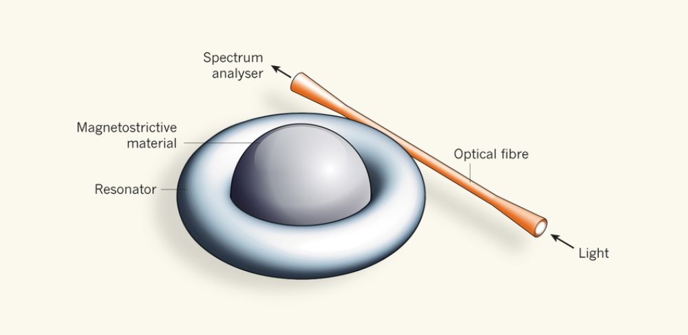
Jörg Wrachtrup & Amit Finkler
Nature 512, 380–381 (28 August 2014) doi:10.1038/512380a
An improved design for a class of magnetometer greatly increases the sensitivity of these devices — and might be the vanguard of a new generation of hybrid sensors that combine different types of signal to increase sensitivity.
When seventeenth-century sailors undertook their dangerous journeys around the Cape of Good Hope or to the Spice Islands, they had an invaluable navigational tool on board: the compass. Only with the aid of this, the most precise measurement device of those times, were they able to accomplish their daring feats. Since then, precision measurements of magnetic fields have been key drivers of basic science and of a whole wealth of technologies with applications ranging from navigation to the medical sciences. Writing in Advanced Materials, Forstner et al. report a vastly improved design for a certain class of magnetometer — a hybrid sensor that measures magnetic fields using an optical signal. …
Figure: An optomechanical magnetometer. Forstner et al. have constructed a magnetic-field sensor in which a doughnut-shaped 'whispering gallery mode' resonator device surrounds a piece of magnetostrictive material. Light is guided through a tapered optical fibre into the sensor, where it is trapped by the resonator. In the presence of a magnetic field, the magnetostrictive material expands, distorting the resonator and changing the frequency at which light resonates in the device. The change of resonance frequency is measured by a spectrum analyser and used to determine the strength of the magnetic field.
… Hybrid sensors thus seem to be an upcoming theme in sensor technology. An important further step will be to use advances in quantum technology to achieve the limits of accuracy. The resulting quantum hybrid sensors could potentially revolutionize sensor technology in various disciplines, enabling unprecedented opportunities in technology and basic science.
Forstner, S. et al. Adv. Mater. http://dx.doi.org/10.1002/adma.201401144 (2014).
Dr. Amit Finkler obtained his bachelor degrees in Electrical Engineering and Physics at Tel Aviv University.
He then moved to the Weizmann Institute of Science, doing his Master's thesis under the supervision of Profs. Amir Yacoby and Eli Zeldov, developing a unique superconducting quantum interference device (SQUID).
In his doctoral thesis, under the supervision of Prof. Zeldov, he worked on a novel scanning SQUID microscope for the study of magnetic phenomena on the nanoscale, which nowadays reaches a single electron spin sensitivity.
After a short interlude in industry in the field of thermoelectrics he moved back to the Weizmann Institute of Science for a post-doctoral position at the atomic scale physics laboratory before arriving in Stuttgart. (Picture: Grafiklabor Physik)
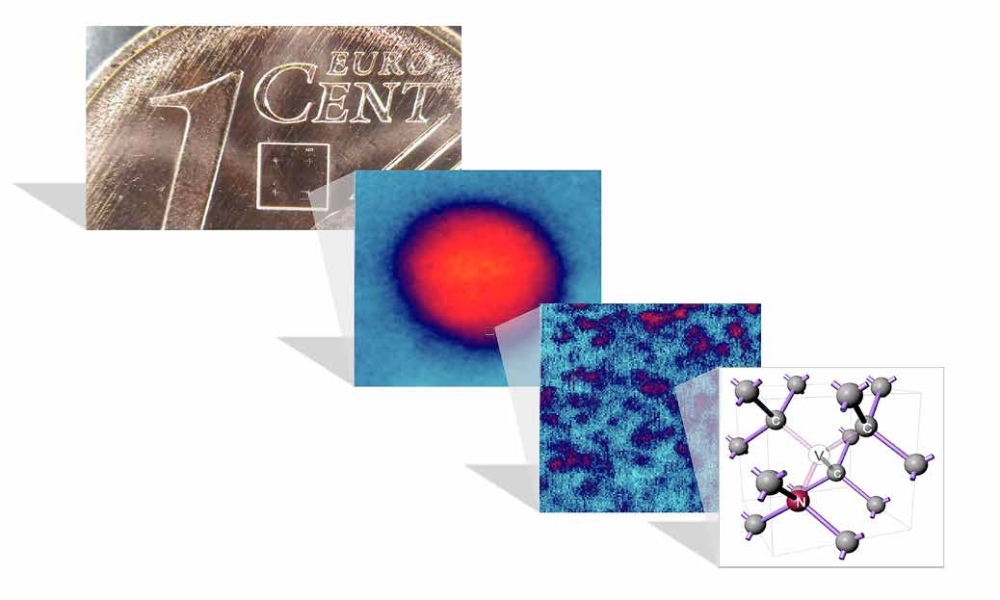
Dieselben Eigenschaften, die Diamanten zu spektakulären Edelsteinen machen, begründen auch ihre hervorragenden Einsatzmöglichkeiten in der Quantentechnologie. Eine Forschergruppe untersucht die quantenphysikalischen Grundlagen des Materials und eröffnet so neue Wege für Halbleitertechnologie, Quanteninformationsverarbeitung und Medizin.
Die meisten Menschen dürften sich beim Betrachten eines Diamanten an den vielfältigen optischen Reflexionen der Facetten des geschliffenen Steins erfreuen. Quantenphysiker, Materialwissenschaftler und Chemiker hingegen machen sich neuerdings gemeinsam Gedanken über die Quantennatur der Diamantbausteine und interessieren sich insbesondere für die in ihnen eingeschlossenen Defekte. Die Forschergruppe „Diamond Materials for Quantum Applications“ mit Teams in Stuttgart, Freiburg, Ulm, Mainz, Leipzig, München, Berlin, Saarbrücken und Würzburg untersucht die außerordentlichen Eigenschaften von Diamant und arbeitet daran, sie gezielt für die Quantenwissenschaften auszunutzen.
Eine mögliche Anwendung dieses Mechanismus liegt in der Quanteninformationsverarbeitung. Hier wird versucht, Quantenmechanische Effekte zu nutzen, um besonders effektiv Informationen verarbeiten zu können. In der Forschergruppe werden dazu die Elektronen und Kerne der Defektzentren als Quantenbits genutzt. Die Ausrichtung der Spins stellt den Wert der Quantenbits dar: Parallel oder antiparallel zum Magnetfeld steht dabei für eine Eins oder eine Null. Quantenbits müssen in einem Zustand existieren, der sowohl Eins als auch Null sein kann, um das volle Potenzial der Quanteninformationsverarbeitung auszuschöpfen. Diese kohärente Überlagerung ist einer der Effekte, der in der Quanteninformationsverarbeitung genutzt wird, um beispielsweise besonders effektive Suchalgorithmen zu entwickeln. Sie ist jedoch labil und wird durch Gitterschwingungen sehr rasch in den jeweils anderen der beiden Eigenzustände – also parallel oder antiparallel zum Magnetfeld – umgewandelt. Die herausragende Härte von Diamant führt aber dazu, dass kaum Gitterschwingungen existieren, die diese Überlagerungszustände beeinflussen könnten. Die Forscherteams in Ulm und Stuttgart setzen diese besondere Qualität von Diamant ein und versuchen, die Defekte für die Quanteninformationsverarbeitung zu nutzen.
Eines der aufsehenerregendsten Anwendungsgebiete der Diamantquantentechnologie ist die Sensorik. Die Stuttgarter Arbeitsgruppe hatte bereits vor einiger Zeit herausgefunden, dass Diamantdefekte äußerst empfindliche Sensoren für Magnetfelder auf der Nanometerskala sind. Besonders ist dabei, dass diese Sensoren ihre Empfindlichkeit unter gängigen Umgebungsbedingungen erreichen. Das macht sie für die Anwendung in den Lebenswissenschaften interessant. Andere Mitglieder der Forschergruppe haben nun gezeigt, dass Diamantdefekte auch empfindliche Sensoren für Temperaturen und elektrische Felder sind. Um die Defekte zu diesem Zweck zu nutzen, werden sie in sehr kleine Diamantkristallite mit wenigen Nanometern Abmessungen verpackt. Weltweit führende Experten für die Herstellung und chemische Modifizierung von Nanodiamanten sind die Mitglieder des Würzburger Forscherteams. Sie stellen Nanodiamanten her, indem sie große, mit Farbzentren dotierte Diamanten der Freiburger Arbeitsgruppe zu Nanodiamanten zermahlen. Aus dem Mahlgut werden sodann die Partikel geeigneter Größe herausgesucht und chemisch modifiziert. Die Nanodiamanten sind mittlerweile ein weltweit nachgefragtes Material, da sie vielfach eingesetzt werden können: Beispielsweise lassen sich die Nanokristalle selbst als Sensoren für zelluläre oder auch medizinische Untersuchungen einsetzen. Indem die Forschergruppe physikalische und materialwissenschaftliche Grundlagenforschung betreibt, liefert sie daher Ergebnisse, die nicht nur für die Quantenphysik, sondern auch für eine Reihe von Anwendungsfeldern von unmittelbarem Interesse sind.
Quelle:
Quanten statt Karat, Prof. Dr. Jörg Wrachtrup, 27 JUN 2014, DOI: 10.1002/fors.201490026
Copyright © 2014 WILEY-VCH Verlag GmbH & Co. KGaA, Weinheim
The Max-Planck-Gesellschaft and the Alexander von Humboldt Foundation honour pioneering work in the field of quantum nanoscience
July 17, 2014: Very special rules apply in the nanoworld – the laws of quantum physics. And because Robert J. Schoelkopf and Jörg Wrachtrup have been exploiting them in a very ingenious way, for example to make headway with quantum information technology, the Alexander von Humboldt Foundation and the Max-Planck-Gesellschaft have decided to honour them this year with the Max Planck Research Award. Robert Schoelkopf researches and teaches at Yale University; he developed qubits from superconducting electronic circuits. Qubits could form the smallest computing units of a quantum computer, which might in future solve various tasks significantly faster than conventional computers. Jörg Wrachtrup is professor at the University of Stuttgart and Fellow of the Max Planck Institute for Solid State Research; with his research on single electrons and nuclear spins in diamonds, he opens up, for example, not only new possibilities in electronics, but also for extremely accurate biological investigations. Each award winner will receive 750,000 euros which may be used to fund research chosen by the award winner as well as collaborative efforts with German or foreign scientists.
The award presentation will take place on November 27, 2014 in Berlin. (PH)
Quelle: MPI
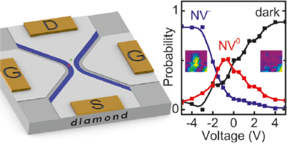
For many applications of the nitrogen-vacancy (NV) center in diamond, the understanding and active control of its charge state is highly desired. In this work, we demonstrate the reversible manipulation of the charge state of a single NV center from NV- across NV0 to a nonfluorescent, dark state by using an all-diamond in-plane gate nanostructure. Applying a voltage to the in-plane gate structure can influence the energy band bending sufficiently for charge state conversion of NV centers. These diamond in-plane structures can function as transparent top gates, enabling the distant control of the charge state of NV centers tens of micrometers away from the nanostructure.
Reference:
Nano Lett. 2014, 14, 2359?2364
Moritz V. Hauf, Patrick Simon, Nabeel Aslam, Matthias Pfender, Philipp Neumann,
Sebastien Pezzagna, Jan Meijer, Jörg Wrachtrup, Martin Stutzmann, Friedemann Reinhard,
and Jose A. Garrido,
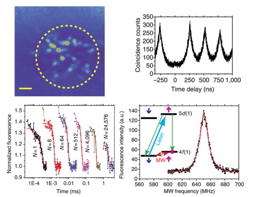
Rare-earth-doped crystals are excellent hardware for quantum storage of photons. Additional functionality of these materials is added by their waveguiding properties allowing for on-chip photonic networks. However, detection and coherent properties of rare-earth single-spin qubits have not been demonstrated so far. Here, we present experimental results on high-fidelity optical initialization, effcient coherent manipulation, and optical readout of a single electron spin of Ce 3+ ion in a YAG crystal. Under dynamic decoupling, spin coherence lifetime reaches T 2 = 2 ms and is almost limited by the measured spin-lattice relaxation time T 1 = 4.5 ms. Strong hyperfine coupling to aluminium nuclear spins suggests that cerium electron spins can be exploited as an interface between photons and long-lived nuclear spin memory. Combined with high brightness of Ce 3+ emission and a possibility of creating photonic circuits out of the host material, this makes cerium spins an interesting option for integrated quantum photonics.
Reference:
P. Siyushev et al. Nature Communications 5, 3895 (2014)
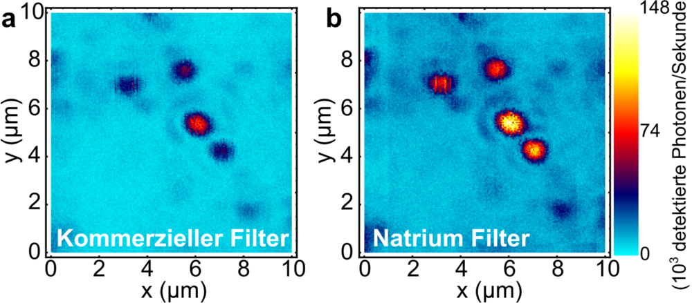
Future quantum communication will rely on the integration of single-photon sources, quantum memories and systems with strong single-photon nonlinearities. Two key parameters are crucial for the single-photon source: a high photon flux with a very small bandwidth, and a spectral match to other components of the system. Atoms or ions may act as single-photon sources—owing to their narrowband emission and their intrinsic spectral match to other atomic systems—and can serve as quantum nonlinear elements. Unfortunately, their emission rates are still limited, even for highly efficient cavity designs. Single solid-state emitters such as single organic dye molecules are significantly brighter and allow for narrowband photons; they have shown potential in a variety of quantum optical experiments but have yet to be interfaced with other components such as stationary memory qubits. Here we describe the optical interaction between Fourier-limited photons from a single organic molecule and atomic alkali vapours, which can constitute an efficient quantum memory. Single-photon emission rates reach up to several hundred thousand counts per second and show a high spectral brightness of 30,000 detectable photons per second per megahertz of bandwidth. The molecular emission is robust and we demonstrate perfect tuning to the spectral transitions of the sodium D line and efficient filtering, even for emitters at ambient conditions. In addition, we achieve storage of molecular photons originating from a single dibenzanthanthrene molecule in atomic sodium vapour. Given the large set of molecular emission lines matching to atomic transitions, our results enable the combination of almost ideal single-photon sources with various atomic vapours, such that experiments with giant single-photon nonlinearities, mediated, for example, by Rydberg atoms, become feasible.
a Recorded lateral scan across the sample with a commercial long-pass filter (594LP).
b The same area, filtering the emission solely with a hot sodium cell. The overall signal rate is increased, and the signal-to-noise ratio is enhanced.
Reference:
Molecular photons interfaced with alkali atoms
Petr Siyushev, Guilherme Stein, Jörg Wrachtrup & Ilja Gerhardt
Nature 509, 66–70 (01 May 2014), doi:10.1038/nature13191
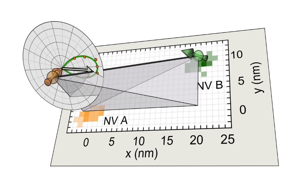
Nanoscale Detection of a Single Fundamental Charge in Ambient Conditions Using the NV- Center in Diamond
Single charge detection with nanoscale spatial resolution in ambient conditions is a current frontier in metrology that has diverse interdisciplinary applications. Here, such single charge detection is demonstrated using two nitrogen-vacancy (NV) centers in diamond. One NV center is employed as a sensitive electrometer to detect the change in electric field created by the displacement of a single electron resulting from the optical switching of the other NV center between its neutral (NV0) and negative (NV-) charge states.
The nanoscale detection of a single fundamental charge allows to gain insight into the charge dynamics of the NV center and its surrounding experiment. E.g. the field data suggests, that the charge is ionized to the conducting band, and not as suggested in other models is transferred to a close by charge trap. This technique therefore allows to gain insight into the local nanoscale charge distribution and opens up a pathway to detect the charge distribution outside of diamond using shallow implanted NV centers or nanodiamonds.
Reference:
Nanoscale Detection of a Single Fundamental Charge in Ambient Conditions Using the NV- Center in Diamond
Florian Dolde, Marcus W. Doherty, Julia Michl, Ingmar Jakobi, Boris Naydenov, Sebastien Pezzagna, Jan Meijer, Philipp Neumann, Fedor Jelezko, Neil B. Manson, and Jörg Wrachtrup
Physical Review Letters 112, 097603 2014 – Published March 3, 2014
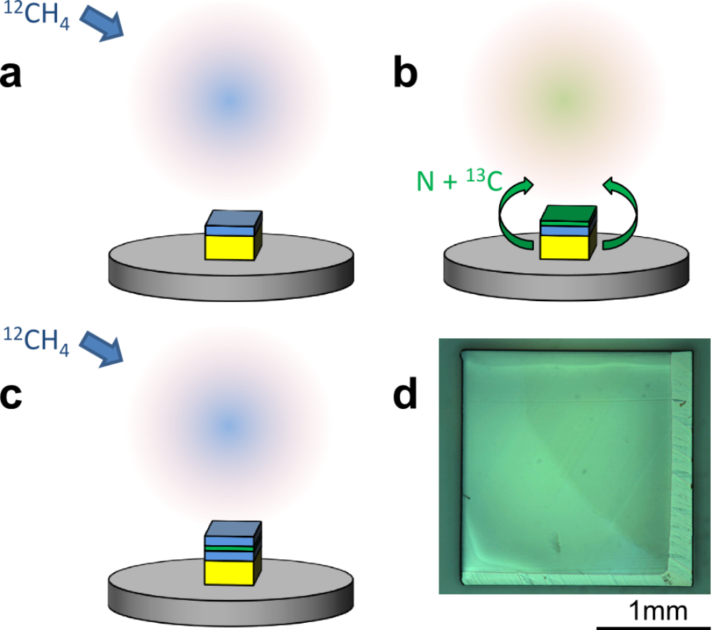
Perfect alignment and preferential orientation of nitrogen vacancy centers during CVD growth of diamond on (111) surfaces
Synthetic diamond production is key to the development of quantum metrology and quantum information applications of diamond.
The major quantum sensor and qubit candidate in diamond is the nitrogen vacancy (NV) color center. This lattice defect comes in four different crystallographic orientations leading to an intrinsic inhomogeneity among NV centers that is undesirable in some applications. In this work, we report a microwave plasma-assisted chemical vapor decomposition (MPCVD) diamond growth technique on (111)-oriented substrates that yields perfect alignment (94 %) of as-grown NV centers along a single crystallographic direction. In addition, clear evidence is found that the majority (74 %) of the aligned NV centers were formed by the nitrogen being first included in the (111) growth surface and then followed by the formation of a neighboring vacancy on top.
The achieved homogeneity of the grown NV centers will tremendously benefit quantum information and metrology applications using identical qubits. In a NV spin ensemble up to 75 % of all spins might be unusable and, worse still, the unusable spins may deteriorate the device performance.
Optically detected magnetic resonance (ODMR) techniques are applied to the NV centers to verify their alignment. Due to refined insight into the NV centers properties the orientation of the N-V pair can now also be determined using the combined application of electric and magnetic fields.
More specifically, ODMR was combined with an axially aligned magnetic field to verify the alignment of the NV centers and ODMR was combined with both transverse magnetic and electric fields to determine the orientations of the NV centers. Such a measurement images the C3v symmetry of the NV center. As the diamond structure was independently determined via x-ray crystallography, the orientation of the NV center could be via the geometry of the diamond lattice.
Fig. 1: The diamond was grown in several steps, as the diamond had to be etched during the growth process (b.) to enable a growth in the <111> direction. During the normal growth process, (a.) and (c.), an C12 isotopic enriched methane flow was used. (d.) shows a Normarski-mode optical microscope image of the fully grown diamond.
Fig. 2: For NVs aligned with the <111> crystal axis, two different orientations are possible, with the nitrogen atom up (red) and down (blue). These two different orientations lead to two 'three-leaves' that are shifted relatively to each other in the spin level shift while rotating a vertical magnetic and electric field.
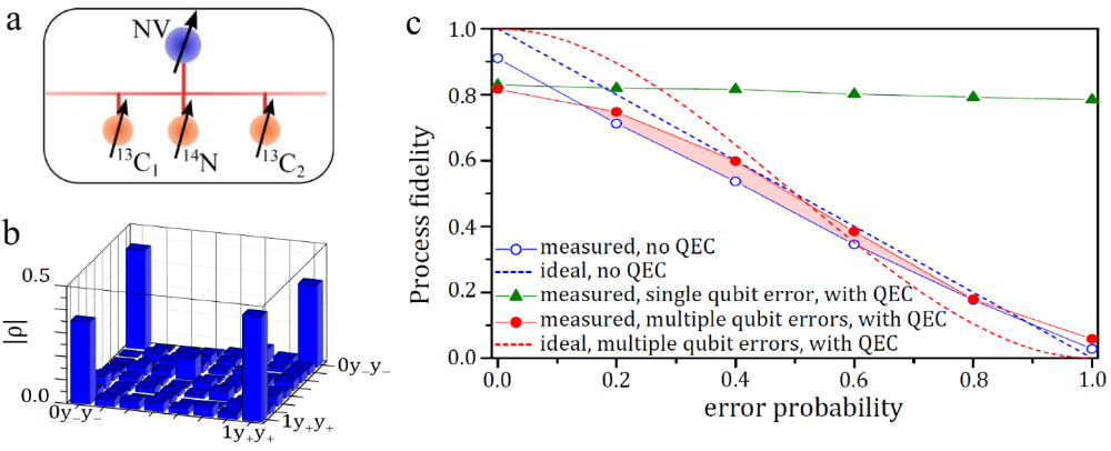
Quantum error correction in a small spin-based quantum computer in diamond
Error correction is a central paradigm in classical and quantum computation. Decoherence caused by the inevitable interaction of quantum bits with their environment leads to dephasing or even relaxation. Correcting the concomitant errors thus is a fundamental requirement for scalable quantum computation. Although algorithms for error correction are known since quite some time experimental realizations are scarce. In this work we demonstrate a high degree of control sufficient for quantum error correction on a hybrid solid-spin system, based on the nitrogen-vacancy defect (NV) in diamond. Nuclear spins randomly distributed within the diamond are addressed, read out and initialized by the electron spin of the defect. The electron spin in turn is polarized and readout by optical means. Specifically, we use three nuclear spins 14 N and two
13 C as quantum bits. All nuclear spins of the register can be individually addressed via their hyperfine interaction, which allows for universal quantum control and quantum computation.
We demonstrate that joint initialization, projective readout and fast local and non-local gate operations are no conflicting requirements in such spin systems, even under ambient conditions. High-fidelity initialization of a whole spin register (99%) and single-shot readout of multiple individual nuclear spins is achieved by using the ancillary electron spin of a nitrogen-vacancy defect. Implementation of a novel non-local gate generic to our electron-nuclear quantum register allows to prepare entangled states of three nuclear spins, with fidelities exceeding 85%. With these techniques, we finally demonstrate three-qubit phase-flip error correction. Utilizing optimal control, all of the above algorithms achieve fidelities approaching fault tolerant quantum operation, thus paving the way to large scale integrations. Besides diamond spins, our techniques can be used to improve scaling of quantum networks relying on phosphorous in silicon, quantum dots, silicon carbide or rare earth ions in solids.
a Illustration of the quantum register consisting of three nuclear spins coupled to the central NV electron spin.
b Reconstructed density matrix for a GHZ-like state within the three nuclear spins.
c Measured process fidelity of the quantum error correction protocol, depending of the error probability.
Reference:
Quantum error correction in a solid-state hybrid spin register.
G.Waldherr, Y.Wang, S. Zaiser, M. Jamali, T. Schulte-Herbrüggen, H. Abe, T. Ohshima, J. Isoya, J. F. Du, P. Neumann, J. Wrachtrup.
Nature (2014) DOI: 10.1038/nature12919
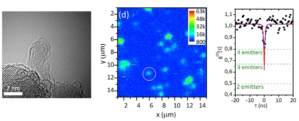
Doping of carbon nanoparticles with impurity atoms is central to their application. However, doping has proven elusive for very small carbon nanoparticles because of their limited availability and a lack of fundamental understanding of impurity stability in such nanostructures.
We present that diamond nanoparticles as small as 1.6 nm, comprising only ~400 carbon atoms, could be extracted from a chondrite (stony, non-metallic meteorite), Efremovka CV3, and they are capable of housing stable photoluminescent color centers, namely the silicon vacancy (SiV). Surprisingly, fluorescence from SiVs is stable over time, and few or only single color centers are found per nanocrystal. We also observe size-dependent SiV emission supported by quantum-chemical simulation of SiV energy levels in small nanodiamonds.
Although these sub-2 nm nanodiamond particles, presumably of presolar origin and older than their parent body (meteorites), exist only in a few cosmochemical laboratories, nanodiamonds in size between 2 and 5 nm have already been produced and our results have the potential to spur further research in producing smaller nanodiamonds.
Our work opens the way to investigate the physics and chemistry of molecular-sized cubic carbon clusters and promises the application of ultrasmall non-perturbative fluorescent nanoparticles as markers in microscopy and sensing.
Left: AC-HRTEM image of free standing ND grain with a size of 2 nm, middle: Confocal fluorescence scan image of the dispersed nanodiamond sample, right: Autocorrelation function showing the background-corrected raw data (black) fitted with a model including the instrument response function (blue) and the found g(2) function (red).
Reference:
Molecular-sized fluorescent nanodiamonds
I. I. Vlasov, A. A. Shiryaev, T. Rendler, S. Steinert, S.-Y. Lee, D. Antonov, M. Voros, F. Jelezko, A. V. Fisenko, L. F. Semjonova, J. Biskupek, U. Kaiser, O. I. Lebedev, I. Sildos, P. R. Hemmer, V. Konov, A. Gali, J. Wrachtrup
Nature Nanotechnology (2013) DOI: 10.1038/NNANO.2013.255
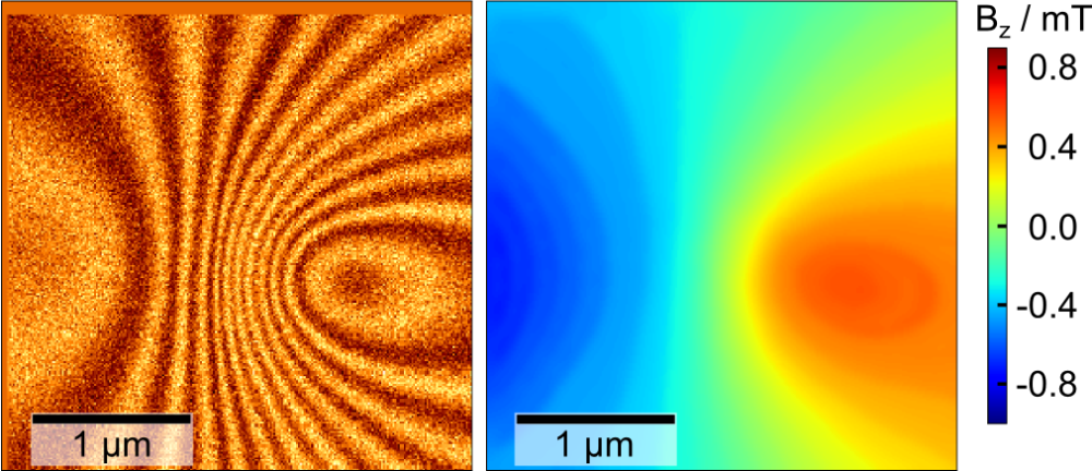
Optimal-control spectroscopy on a scanning qubit reveals multiple contour lines of the magnetic field in a single scan.
Microscopes able to image magnetic fields are an increasingly important tool, not only for material physics but also for industry where they are used to check the magnetic field of hard disk write heads.
The NV center in diamond – an atomic-size color defect – is a promising candidate for the next generation of sensor heads for magnetic field microscopes. It can sense magnetic fields with high (nT) sensitivity and, more importantly, sub-nm resolution. This latter property is an order of magnitude better than existing techniques such as magnetic force microscopy.
Imaging of magnetic fields with NV centers has been demonstrated before, but has so far required sophisticated and error-prone control techniques (e.g. lock-in detection). We now managed to radically simplify this technique with the help of a computer-optimized spectroscopy protocol based on a technique known as optimal control. Our protocol switches off fluorescence of a scanning color center whenever the magnetic field reaches one of several magic values. Scanning through a spatially varying magnetic field, fluorescence of the center simultaneously images multiple contour lines of the magnetic field – lines where the field takes on one of the magic values. This pattern is visually and conceptually analogous to tree lines in biology, which – mathematically phrased – reveal all parts of a piece of wood that were grown by the tree at a particular instant in time.
Technically, this contour line pattern can be used to quantitatively reconstruct a map of the full magnetic field, just as tree-rings can reveal the growth history of a tree.
We demonstrated our technique by imaging a MFM-tip as an example of a magnetic nanostructure, gaining previously unknown insights into the magnetic field structure of the MFM-tip, which was then used to check different models of the MFM-tip's magnetic field for validity.
Reference:
High-Dynamic-Range Imaging of Nanoscale Magnetic Fields Using Optimal Control of a Single Qubit
Phys. Rev. Lett. 111, 170801 (2013)
Thomas Häberle, Dominik Schmid-Lorch, Khaled Karrai, Friedemann Reinhard, and Jörg Wrachtrup
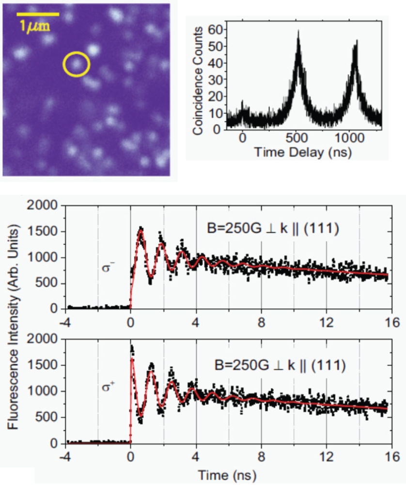
Mapping Spin Coherence of a Single Rare-Earth Ion in a Crystal onto a Single Photon Polarization State
We report on optical detection of a single photostable Ce 3+ ion in an yttrium aluminium garnet (YAG) crystal and on its magneto-optical properties at room temperature. The spin quantum state of the emitting level of a single cerium ion in YAG can be initialized by circularly polarized laser pulse. Coherent precession of the electron spin is read out by observing temporal behaviour of circularly polarized fluorescence of the ion. This implies direct mapping of the spin quantum state of Ce 3+ ion onto the polarization state of the emitted photon and represents quantum interface between a single spin and a single photon.
Reference:
Mapping Spin Coherence of a Single Rare-Earth Ion in a Crystal onto a Single Photon Polarization State
Phys. Rev. Lett. 111, 120502 (2013)
Roman Kolesov, Kangwei Xia, Rolf Reuter, Mohammad Jamali, Rainer Stöhr, Tugrul Inal, Petr Siyushev, and Jörg Wrachtrup
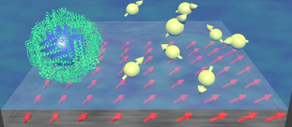
Sensing and imaging paramagnetic species under physiological conditions is a key technology in chemical and biochemical analytics, cell biology, and medical sciences. At submicrometer length scales, nitrogen-vacancy (NV) centers in diamond offer atom-sized probes for magnetic fields. We show that spin relaxation of an ensemble NV sensor allows sensing of adsorbed and freely diffusing manganese(II) ions and adsorbed ferritin. Sensitivities approach 175 Mn ions and 10 ferritin proteins per diffraction limited spot under ambient conditions.
Citation:
“Highly Sensitive Detection of Physiological Spins in a Microfluidic Device”
Ziem, F. C., Götz, N. S., Zappe, A., Steinert, S. & Wrachtrup, J., Nano letters (2013). doi:10.1021/nl401522a
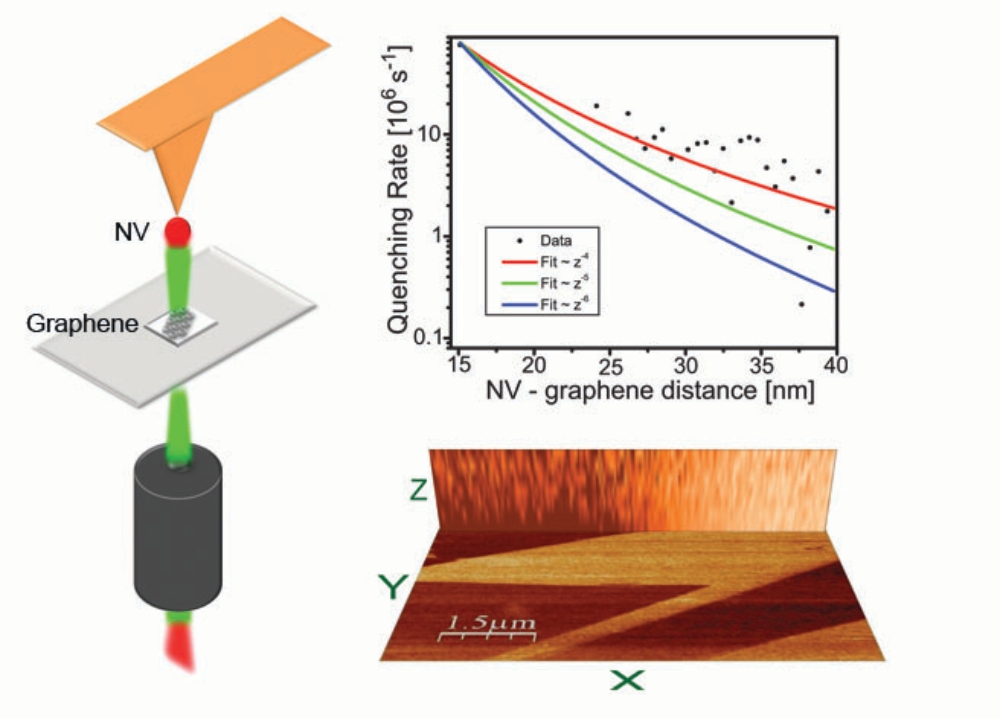
Single Defect Center Scanning Near-Field Optical Microscopy on Graphene
We present a scanning-probe microscope based on an atomic-size emitter, a single nitrogen-vacancy center in a nanodiamond. We employ this tool to quantitatively map the near-field coupling between the NV center and a flake of graphene in three dimensions with nanoscale resolution. Further we demonstrate universal energy transfer distance scaling between a point-like atomic emitter and a two-dimensional acceptor. Our study paves the way toward a versatile single emitter scanning microscope, which could image and excite molecular-scale light fields in photonic nanostructures or single fluorescent molecules.
Reference:
Single Defect Center Scanning Near-Field Optical Microscopy on Graphene”
J. Tisler, et al., Nano Lett., 2013, 13 (7), pp 3152–3156, DOI: 10.1021/nl401129m
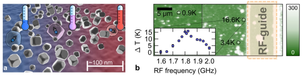
The precise measurement of temperature is a vital characterization tool in material and life sciences. However, at the length scale of for example state-of-the-art silicon technology or intracellular organelles only a few thermometers exist and their accuracy is often insufficient to monitor processes of interest.
We have developed a novel temperature sensor which combines high accuracy and high spatial resolution at the same time. To this end we have exploited the temperature response of a single quantum system inside the diamond lattice, namely the nitrogen-vacancy (NV) center.
Nanodiamonds form rigid and protective cages for defects like the NV center which can be used as versatile sensor probes, either attached to scanning devices, like atomic force microscopes, or dispersed on or inside a sample. Their small sizes (~10 – 100 nm) allow measurements on the nanometer scale. The electronic spin associated with the NV center in diamond is sensitive to many influences from its environment, for example magnetic and electric fields. Using a new technique now also allows to measure temperature with high accuracy, without having to modify the nanodiamond probe.
Changes in the temperature affect the transition frequencies of the NV spin. This effect is usually hidden as other effects, mostly magnetic fields, dominate the spin dynamics. In order to reveal the influence of the temperature, a new decoupling technique was devised. It cancels out effects arising from magnetic fields, but retains the temperature influence. In addition the diamond quality was improved substantially to reduce deleterious effects of lattice impurities.
This way a temperature sensor with an accuracy of 1 mK and a sensitivity of 5 mK/Hz½ was realized. Using dispersed nanodiamonds on a glass slide (Fig. a), we could measure the temperature gradient close to an operational microstructured resonator in the range of a few micrometers (Fig. b).
Our novel method could yield applications in material and life sciences. One could for example imagine tracking temperature changes during the metabolism of a living cell.
This research was a joint effort of the Universities of Tsukuba (Japan), Dortmund and Stuttgart and the company Sumitomo.
Figure a: Schematics of dispersed nanodiamonds. Typical scales are in the range of tens to hundreds of nanometers. Single nanodiamonds containing NV centers can be used as individual temperature probes.
Figure b: The temperature gradient near a heated RF-guide is measured with dispersed nanodiamonds.
Reference:
“High-Precision Nanoscale Temperature Sensing Using Single Defects in Diamond”
P. Neumann, et al., Nano Lett., 2013, 13 (6), pp 2738–2742
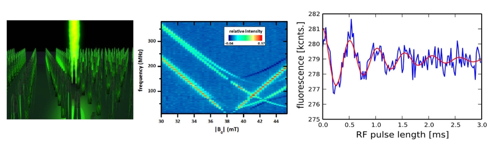
Initialization and readout of a single nuclear spin with a meta-stable electron spin ancilla
Electron spins in solids have been considered as one of promising candidates for solid state quantum qubit because their spin states can be well detected – even on the single spin level – either electrically or optically owing to their abilities to strongly interact with electrical charges and optical photons. Because the initialization and readout process can limit the coherence of such delicate quantum object, hybrid quantum systems consisting of electron and nuclear spins have been proposed. While the electron spins usually are used for readout, the quantum information can be stored in the nuclear spins which usually have longer coherence time.
The coupling between electron and nuclear spins in this hybrid quantum system is essential for readout and transfer of quantum information. It can, however, meditate the electron-nuclear spin flip-flops which also limits nuclear spin coherence. This has motivated searching for new spin systems in which the nuclear spins can be decoupled during the storage process. A spin system which has a spin-free ground state can be a favorable one [1].
For our study, a newly found color center in diamond nano-wires, the ST1 center, has been used. This new color center has an electronic singlet ground state and a meta-stable triplet state and shows exceptionally high (up to 45 %) optical spin signal contrast. The strong coupling between the metastable electron spin and a nearby nuclear spin is used for the initialization of the nuclear spin memory which is then stored for at least 1 ms at room temperature, while the electronic spin decays to the singlet ground state [2]. Even though the memory time is currently limited by either intrinsic nuclear spin bath decoherence or paramagnetic impurities in nano-wires, this study demonstrates that nuclear spins coupled to single metastable electron spins are useful quantum systems with potentially long memory times.
Left: An illustrative image showing diamond nano-wires coupled to green Laser light, middle: Optically detected resonance transitions of a metastable electronic triplet spin of a single ST1 center coupled to a 13C nuclear spin. Some transitions get weaker because of the optical nuclear polarization induced by the level anti-crossing around 42 mT, right: the observed nuclear spin Rabi oscillation at dark condition.
[1] V. Filidou et al., Nat. Phys 8, 596 (2012).
[2] S.-Y. Lee et al., arXiv:1302.4608 (2013), to be published in Nat. Nano.
Photo-induced ionization dynamics of the nitrogen vacancy defect in diamond investigated by single-shot charge state detection
The properties of the negatively charged nitrogen vacancy (NV) defect are usually exploited in various applications like magnetic field sensing and quantum information processing. However, the NV center in diamond can also occur in the neutral charge state (NV0). It has been shown that upon illumination (532 nm) a continuous ionization and recombination process of the NV defect is going on. This charge state dynamics was examined in detail in the present work utilizing different methods. Emphasis was on the excitation wavelength dependence.
In this study it was experimentally proven that a recently observed “dark” state of the negatively charged NV defect is indeed its neutral charge state. The rates of the ionization and recombination processes were measured for a broad range of excitation wavelengths. It was determined which wavelengths are optimum to gain maximum NV minus population. Additionally, the transition from a two-photon ionization process to a one-photon ionization process was observed by varying the excitation laser light from the green to the blue spectral range. This change in the ionization process revealed the energy level of the ground state of NV minus within the bandgap of diamond.
The work gives new insight into the photophysics of the NV defect. The detailed study of the charge state switching behavior allows for implementation of methods like Photoactivation Localization Microscopy (PALM) or Stochastic Optical Reconstruction Microscopy (STORM) with NV centers. This enables the resolution of single NV centers with distances well below the diffraction limit.
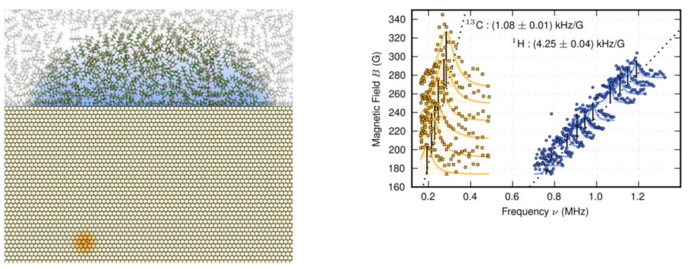
Science 339, 561 (2013)
A new diamond based sensor is small and sensitive enough to probe the nuclear magnetic resonance (NMR) signal of a nanoscale sample volume. NMR is an interesting effect, in which information about a sample’s structure can be extracted by detecting the weak magnetic fields of certain atomic nuclei, such as hydrogen. It is well known for its application in clinical Magnetic Resonance Imaging (MRI), and is widely used in experimental science as well, but extensions to nanoscale samples have remained an elusive goal due to the insensitivity of conventional detection methods. The new diamond sensor overcomes these restrictions and paves the way towards “nanoMRI”.
NMR and MRI measurements on the nanoscale have been done so far only using magnetic force resonance microscopy (MRFM), a challenging experimental technique operating at low temperature in vacuum. The new approach utilizes a near-surface single nitrogen-vacancy (NV) center in diamond as a novel atomic size magnetic field sensor and functions even under ambient conditions.
The NV center gives the diamond a red fluorescent glow, which can be bright or dull depending on which way the NV’s electrons are spinning. Varying liquid and plastic samples were placed on the diamond surface and the weak magnetic field of the samples hydrogen spins interacts with the electrons of the NV center. The magnetic field of the hydrogen nuclei was detected by coherently manipulate the NV and looking onto its fluorescence. The sensor performance reaches voxel sizes down to (5nm) 3.
An important extension of this result will be the combination with a scanning probe setup, to implement NMR imaging on the nanoscale, potentially enabling the structural analysis of single molecules.
a) visiualization of the experimental setup – a single shallow NV center (red spot) allows for the detection of the weak magnetic field of hydrogen nuclei in a nanoscale sample volume (colored drop, upper figure half). b) NMR spectrum of the detected nuclei in the vicinity of the NV center. A strong contribution from the intrinsic 13 C inside the diamond (yellow) is accompanied by a weaker component of the 1 H nuclei of the sample (blue). Both components shift with the magnetic field at the gyromagnetic ratios of the respective spin species.
Nuclear Magnetic Resonance Spectroscopy on a (5-Nanometer) 3 Sample Volume
Staudacher, T., Shi, F., Pezzagna, S., Meijer, J., Du, J., Meriles, C. A., Reinhard, F. & Wrachtrup, J. Science 339, 561 (2013)
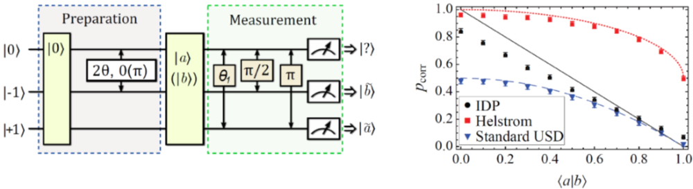
Due to imperfections, real measurements on quantum systems are seldom ideal projective measurements. Moreover, it is sometimes advantageous to deliberately design a quantum measurement that is not projective, depending on exactly what property of the measured quantum system one is interested in. One example is when distinguishing between non-orthogonal quantum states. This is not possible to achieve perfectly with certainty, but can be optimized with respect to two aspects: One the one hand, the probability the get a correct result can be maximized, which is the so called Helstrom measurement. On the other hand, the measurement can be unambiguous, such that each result is correct, at the expense of having inconclusive results. This is the so called Ivanovic-Dieks-Peres (IDP) measurement. This type of measurement is relevant for important quantum information tasks in quantum cryptography and in entanglement swapping protocols. Moreover, it can be useful for quantum communication, when the two signal states are non-orthogonal after passing through a channel.
Here, we present and compare experimental realizations of optimal quantum measurements for distinguishing between two non-orthogonal quantum states encoded in a single nuclear spin associated with the nitrogen vacancy defect in diamond. This is the first solid state based implementation of this type of measurement. The figures show the pulse sequence for the IDP measurement, and the probability to obtain a correct result, in dependence of the overlap of the two non-orthogonal states, for the Helstrom, IDP, and standard non optimal measurement.
Distinguishing between Nonorthogonal Quantum States of a Single Nuclear Spin
Gerald Waldherr, Adetunmise C. Dada, Philipp Neumann, Fedor Jelezko, Erika Andersson, and Jörg Wrachtrup
Phys. Rev. Lett. 109, 180501 (2012)
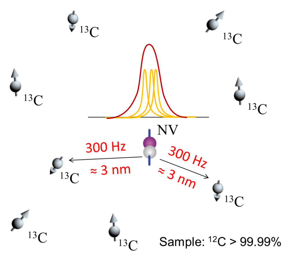
13C nuclear spins coupled to an NV center are a valuable resource for realizing long lived solid state quantum registers. However, the number of nuclear spins that are addressable is limited by the inhomogeneous linewidth of the magnetic resonance transition, which is in turn limited by the nuclear spin bath. If we could address a nuclear spin that is hidden in the broadened resonance line - i.e. the hyperfine coupling is much smaller than the inhomogeneous linewidth - the number of addressable nuclear spins would greatly increase. In this work we demonstrate that this is possible by dynamically decoupling the electron spin from the surrounding nuclear spin bath. By carefully tuning the direction and strength of an applied magnetic field, the electron spin couples selectively only to specific bath spins. Thereby, we can map out the otherwise hidden nuclear spins around an NV center. Using isotopically enriched diamond (99.99% 12C), our method is capable of detecting nuclear spins coupled as weak as 300 Hz.
Further details:
N. Zhao et al. Nature nanotechnology 152 (2012) doi:10.1038/nnano.2012.152
Looking at individual fundamental building blocks of nature, like atoms and molecules, is always intriguing though challenging task. Detecting individual ions of rare-earth elements in laser crystals is such a challenging task because they yield very low light output when illuminated with a laser. At the same time, these ions, if detected, could become excellent quantum bits (qubits) for quantum computer. Recently, we succeeded in detection of single ions of one rare-earth species, namely praseodymium, in an artificial gem-stone yttrium aluminum garnet crystal and in nanometer sized particles of that crystal. The most peculiar feature of praseodymium ions is that they can emit an ultraviolet light once illuminate with a blue laser. We have shown that this ultraviolet radiation can strongly affect the environment in close proximity to the emitting ions. In particular, we have demonstrated that cancerous cells die because of this radiation and that the emitted ultraviolet can expose photosensitive chemicals like photoresists used in chip production. Thus, apart from potential use in quantum computers, the discovered single rare-earth ions might become valuable additions to modern nano- and biophotonics.
Further details:
Optical detection of a single rare-earth ion in a crystal
R. Kolesov et al. Nature Communications 3, 1029 doi:10.1038/ncomms2034
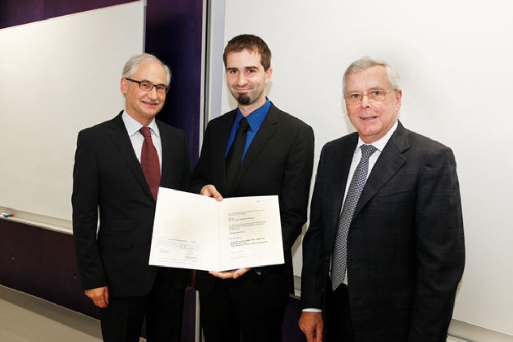
The University of Stuttgart annually awards a prize to the three best PhD thesis of the year. This year Philipp Neumann is among the recipients. Philipp received the prize for his outstanding work on diamond quantum spintronics which resulted in several high profile publications over the past years. He for example for the first time demonstrated electron nuclear spin entanglement in diamond defect spin systems, showed coupling among spin impurities and single shot readout of a nuclear quantum state. In addition Philipp was awarded the annual thesis prize of the collaborative research center SFB/TR21 which has provided the funding for his thesis.

Quantum effects have fascinated physicists for over 100 years, but their study is experimentally challenging for one major reason. Quantum coherence is fragile and breaks once the quantum system under study is “observed”. Interestingly, the “observation” of a quantum system does not require human interaction. Instead, it can be performed by the system's environment, e.g. by the omnipresent electrons, photons, nuclei or atoms. This effect, known as decoherence, has been suggested as an explanation for the measurement problem, which lies at the heart of many quantum paradoxa and most prominently Schrödinger's cat.
In practice, the study of quantum systems is complicated by another challenge. Quantum coherence is extremely sensitive to external noise, such as magnetic or electric fields. This fact is turned into an advantage in atomic accelerometers and magnetometers, where the highly sensitive quantum systems provide excellent sensors. However, it is a serious problem for quantum computers and atomic clocks, the performance of which can be easily spoiled by the stray field of a nearby subway or radio station which breaks their coherence.
These two challenges – exposure to the observation by the environment and to classical noise – have long been regarded as entirely different effects, the former as a fundamental one and the latter merely as an experimental complication. In a recent study [1] we show that they are fundamentally linked and can be regarded as limiting cases of strong and weak coupling to the environment, respectively. We experimentally prove this view by studying an NV center in diamond. It has long been known that this system loses its coherence when it is “observed” by the nuclear spins of the surrounding carbon atoms in the diamond lattice [2]. However, the loss of coherence can equally be explained by a purely classical mechanism: nuclei have a magnetic moment and can thus be considered as a source of classical spin noise, a permanently fluctuating magnetic field.
We demonstrated that this spin noise is indeed indistinguishable from classical magnetic field noise (such as a radio station) if the coupling of the nuclei to the NV center is weak. Moreover, we managed to vary the strength of the coupling and thus to continuously tune the system into the regime of either strong coupling and quantum decoherence or weak coupling and classical spin noise.
[1] Friedemann Reinhard et.al., Phys.Rev.Lett. 108, 200402 (2012)
[2] Lilian I. Childress et.al., Science 314, 281 (2006)
Single-photon sources that provide non-classical light states on demand have a broad range of applications in quantum communication, quantum computing and quantum metrology. Meanwhile, single-photon emission stimulated by optical laser excitation has been demonstrated for a large variety of single quantum systems like atoms, ions, molecules, diamond color centers and semiconductor quantum dots. However, from a technical point of view it is desirable to generate single photon emission by electrical excitation as it was successfully demonstrated for the first time in 2002 using single InAs quantum dots incorporated in a GaAs diode structure. However, a major obstacle of this approach is the requirement of cryogenic temperatures necessary for electrical operation due to the confinement of charge carriers inside the quantum dot at elevated temperatures.
In this context, we were able to design a novel diamond based p-i-n device which proved that the realization of a stable, electrically driven single-photon source from a single neutral nitrogen-vacancy center at room-temperature is feasible. By the demonstration of electroluminescence from a single, neutral NV center an additional central element was added to the quantum toolbox of diamond defects which thereby offers new opportunities in terms of integrating single-photon sources based on diamond defects into electronic control circuitry and spintronic applications for quantum communication and processing. Remarkably, the generation of electroluminescence follows kinetics fundamentally different to that of photoluminescence with intra-bandgap excitation. This phenomenon suggests that the electroluminescent process comprises of a precursor state during electron-hole recombination at the defect site which functions as a rate limiting step in consecutive reactions. A tentative explanation could be drawn from ab ignition calculations in which this additional state is attributed to a loosely bound hole in the valence band edge and a strongly bound electron at the NV center.
Our results thereby show the feasibility of generating single photon emission by electrical excitation at room temperature using single NV centers in the diamond lattice and further highlights that functional single defects can be integrated into electronic control structures, which is a crucial step towards elaborate quantum information devices.
Electrically driven single-photon source at room temperature in diamond
Nature Photonics 10.1038/NPHOTON.2012.75
N. Mizuochi 1,2, T. Makino 3,4, H. Kato 3,4, D. Takeuchi 3,4, M. Ogura 3,4, H. Okushi 3,4, M. Nothaft 5, P. Neumann 5, A. Gali 6,7, F. Jelezko 8, J. Wrachtrup 5 and S. Yamasaki 3,4
1 Graduate School of Engineering Science, Osaka University 1-3, Machikane-yama, Toyonaka-city, Osaka, 560-8531, Japan
2 JST PRESTO, 4-1-8 Honcho Kawaguchi, Saitama, 333-0012, Japan
3 Energy Technology Research Institute-National Institute of Advanced Industrial Science and Technology, Tsukuba, Ibaraki 305-8568, Japan
4 JST CREST, 4-1-8 Honcho Kawaguchi, Saitama, 333-0012, Japan
5 3rd Physics Institute and Research Center SCoPE, Pfaffenwaldring 57, D-70550 Stuttgart, Germany
6 Institute for Solid State Physics and Optics, Wigner Research Centre for Physics, Hungarian Academy of Sciences, Budapest, PO Box 49, H-1525, Hungary
7 Department of Atomic Physics, Budapest University of Technology and Economic, Budafoki ut 8, H-1111 Budapest, Hungary
8 Institut für Quantenoptik, Universität Ulm, Albert Einstein Allee 11, D-89069 Ulm, Germany
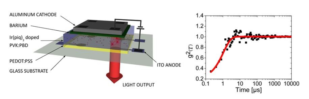
Single-photon emitters have been considered for applications in quantum information processing, quantum cryptography and metrology. For the sake of integration and to provide an electron photon interface, it is of great interest to stimulate single-photon emission by electrical excitation as it was demonstrated for quantum dots in 2002. Because of low exciton binding energies, it has so far not been possible to detect sub-Poissonian photon statistics of electrically driven quantum dots at room temperature. However, organic molecules possess exciton binding energies on the order of 1 eV, thereby facilitating the development of an electrically driven single-photon source at room temperature in a solid-state matrix. However, the choice of an appropriate molecular dopant for electrical excitation experiments is a non-trivial issue. In contrast to molecular photoexcitation experiments in which one usually chooses molecules with a high fluorescence quantum yield and low intersystem crossing probabilities (e.g. Terrylene in p-Terphenyl), in electroluminescence it is necessary to employ a molecular emitter which is able to emit photons using phosphorescence. This requirement results due to the underlying recombination statistics in organic light emitting devices which lead to a probability of 75% to excite the molecule’s triplet state and of 25% to excite the respective singlet state. For a molecule to be able to generate efficient phosphorescent emission, a heavy metal ion needs to be inserted into the molecular structure thereby increasing spin-orbit coupling and reducing the molecule’s triplet state radiative lifetime down to 1 µs. In this work, the organometallic complex Ir(piq) 3 emitting at 615 nm was used as phosphorescent dopant.
By applying low work function barium metal contacts, oxygen-free processing and efficient encapsulation techniques, we were able to design an organic light emitting device with spatial and temporal stable electroluminescence characteristics enabling the demonstration of non-classical electroluminescent emission originating from a single, electrically driven molecule at room temperature.
Electrically driven photon antibunching from a single molecule at room temperature
Nature Communications 10.1038/NCOMMS.1637
M. Nothaf t 1, S. Höhla 2, F. Jelezko 3, N. Frühauf 2, J. Pflaum 4 and J. Wrachtrup 1
1 3rd Physics Institute and Research Center SCoPE, University of Stuttgart, 70550 Stuttgart, Germany
2 Institute for Large Area Microelectronics and Research Center SCoPE, University of Stuttgart, 70550 Stuttgart, Germany
3 Institute for Quantum Optics, University of Ulm, 89069 Ulm, Germany
4 Experimental Physics VI, University of Würzburg and ZAE Bayern, 97074 Würzburg, Germany
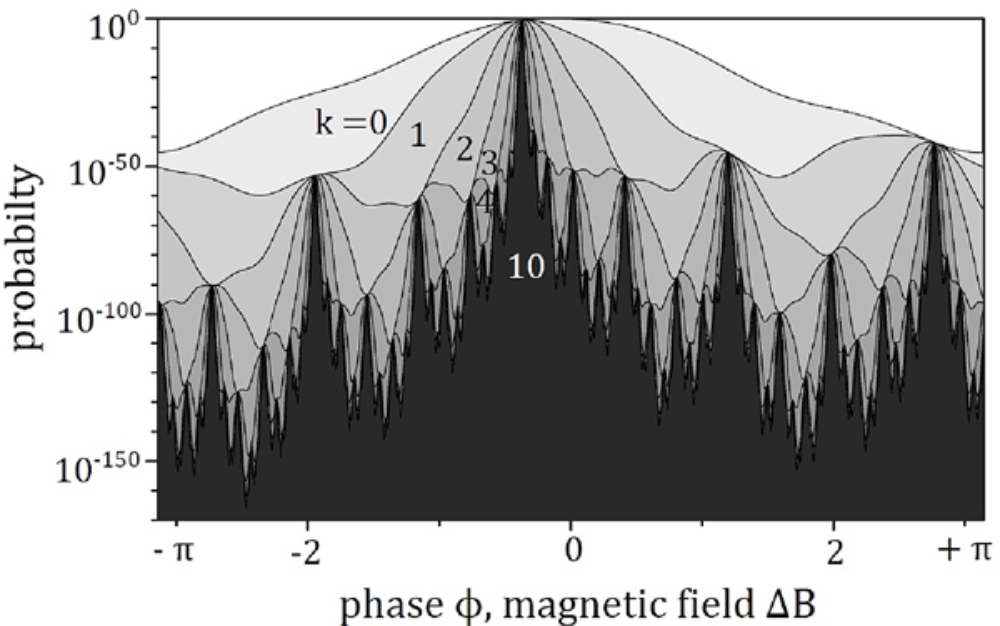
One main application of the nitrogen-vacancy defect in diamond is a sensor which can detect weak magnetic and electric fields at the nanoscale. This is done by measuring the field dependent shift in the Lamor frequency of the spin states using Ramsey interferometry: First, a ?/2 pulse creates a superposition of two spin states. The phase of this superposition will then undergo so called Ramsey oscillations, i.e. it will evolve periodically from 0 to 2? with a field dependent frequency. After a certain phase accumulation time, a second ?/2 pulse maps the accumulated phase onto spin state population, which is then measured. From the measurement result, one can deduce the accumulated phase, the Lamor frequency, and the applied field. However, due to the periodic modulation of the phase, such a measurement is ambiguous, which means that the applied field must be known within certain limits to unambiguously determine its value. Effectively, this limits the dynamic range of the sensor.
On the one hand, these limits are less severe for shorter phase accumulation times. On the other hand, longer phase accumulation times lead to a higher measurement precision, even for the same amount of total measurement time: By repeating a measurement with phase accumulation time τ for n times, the precision of the result scales as 1/ τ⋅n 0.5, whereas the precision of a single measurement with phase accumulation time n⋅τ scales as 1/n⋅τ. By using a recently proposed phase estimation algorithm, we combined short, unambiguous measurements with long, high precision measurements. The performance of the algorithm can be seen in the Figure, which shows the probability that a certain phase (which depends on the applied field) was accumulated. For short phase accumulation times (bright region), the distribution is broad but has an unambiguous maxima. As measurements with longer phase accumulation times are included (darker regions), this maxima becomes more narrow.
With this algorithm, we achieved a precision scaling of a magnetic field measurement of T -0.85. For high precision measurements, the dynamic range of the sensor was thereby increased by a factor of 130.
High-dynamic-range magnetometry with a single nuclear spin in diamond
Nature Nanotechnology 10.1038/nnano.2011.224
G. Waldherr 1, J. Beck 1, P. Neumann 1, R. S. Said 2, 3, M. Nitsche 1, M. L. Markham 4, D. J. Twitchen 4, J. Twamley 2, F. Jelezko 1, 5 and J. Wrachtrup 1
1 3. Physikalisches Institut, Research Center SCOPE, and MPI for Solid State Research, University of Stuttgart, Pfaffenwaldring 57, 70569 Stuttgart, Germany,
2 Centre for Engineered Quantum Systems, Department of Physics & Astronomy, Faculty of Science, Macquarie University, Sydney, NSW 2109, Australia,
3 Institut für Quanten-Informationsverarbeitung, Universität Ulm, 89081 Ulm, Germany,
4 Element Six Ltd, King’s Ride Park, Ascot SL5 8BP, UK,
5 Institut für Quantenoptik, Universität Ulm, 89073 Ulm, Germany.
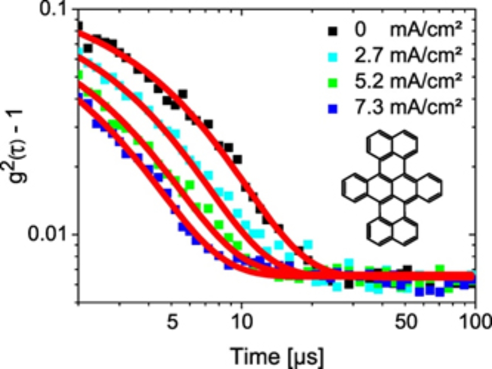
In the light of increased commercial and scientific applicability of organic electronic circuitry and in particular organic light emitting diodes (OLEDs), it is of great interest to study fundamental electrical excitation processes and charge carrier dynamics on molecular length scales. Single molecule studies thereby offer the possibility and material compatibility to perform measurements on the level of a single quantum object in organic electronic devices. By doping of single Dibenzoterrylene (DBT) guest molecules into the charge carrier recombination zone of polymeric OLEDs, we were able to demonstrate that a single fluorescent dopant can be used as nanoscale sensor for current densities with nanometer spatial resolution.
While monitoring laser induced photoluminescence of a single DBT molecule during current injection into the emissive layer of a PPV based OLED, we observed that the PL intensity decreases with increasing current density. In contrast to optical laser excitation, electron-hole recombination mechanisms on a single molecule result in a probability of 75% to excite the triplet state manifold compared to only 25% of singlet state stimulation. This phenomenon is related to spin statistics of two recombining fermionic particles (electron and hole) resulting in either a spin 0 or spin 1 exciton. Therefore, electron-hole recombination processes in organic matrices result in a predominant pumping to the molecule’s dark and long living triplet state which leads to a reduction of photoluminescence intensity with increasing recombination rate and current density. Related to the dielectric constant of the polymer matrix, charge carriers only recombine on a single molecular dopant once they are as close as 17 nm to the dopant. Therefore, by measuring voltage dependent single molecule quenching behaviors, a determination of current densities within the molecular environment, or capture cross section, of the molecular sensor is possible. By the study of photon correlations during charge injection it is further possible to measure current densities solely by optical means without the need of any ampere meter.
In contrast to conductive AFM techniques, this approach thereby enables the non-invasive determination of current densities on nanometer length scales in operational OLED devices.
Optical Sensing of Current Dynamics in Organic Light-Emitting Devices at the Nanometer Scale
CHEMPHYSPHEM 10.1002/cphc.201100442
M. Nothaft 1, S. Höhla 2, A. Nicolet 3, F. Jelezko 4, N. Frühauf 2, J. Pflaum 5, J. Wrachtrup 1
1 3rd Physics Institute and Research Center SCoPE, University of Stuttgart, 70550 Stuttgart (Germany)
2 Institute for Large Area Microelectronics and Research Center SCoPE, University of Stuttgart, 70550 Stuttgart (Germany)
3 Laboratoire National des Champs Magnétiques Intenses, 38042 Grenoble (France)
4 Institut für Quantenoptik, University of Ulm, 89069 Ulm (Germany)
5 Experimentelle Physik VI, University of Würzburg and ZAE Bayern, 97074 Würzburg (Germany)
Prof. Carlos Meriles is visiting the institute as a Humboldt fellow for the upcomming year. Carlos is a specialist in spin physics with major contributions in the field of NMR and single spin physics. He graduated from Universidad Nacional de Cordoba and spent his post doc with Alex Pines in UC Berkeley. Currently Carlos is a professor of physics at City College New York – CUNY. Recently he worked on nuclear induced Faraday rotation, optical spin pumping in GaAs and NV center spin physics. Carlos will spend one year at the institute funded by the Humboldt foundation working on field sensing with diamond spin systems.
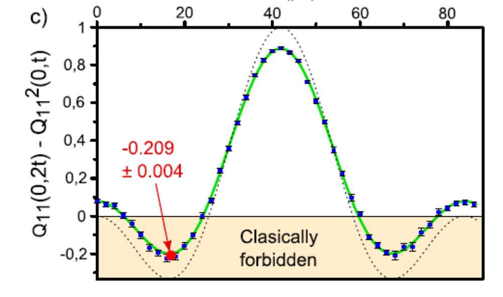
Among the most puzzling aspects of quantum physics is the measurement process being most drastically posed by Schrödinger’s cat paradox. Schrödinger envisaged a (quantum) cat trapped inside a box equipped with some device which may, randomly, kill the cat. Quantum mechanics tells us that at any time, if unobserved, the cat is both dead and alive. However, if the system is probed, for instance by opening the box, we will find the cat in one of the two possible states, either alive or dead. According to the formalism of quantum mechanics, this result is nondeterministic; i.e. the outcome of our measurement – and therefore the (classical) state of the
cat – is not even defined before opening the box. But how can we know that quantum mechanics is not simply incomplete, and that there are not other ‘‘hidden’’ variables on which the state of the cat depends, thus rendering the measurement deterministic? When formulated in the context of spatially separated subsystems, this type of argument leads to the celebrated Bell’s inequality, which limits the strength of the statistical correlations between distant subsystems within a local realistic theory. On the other hand, in contexts where locality is not relevant, the focus is on the premises of realism and the characterization of the type of temporal (vs spatial) correlations that would emerge within this realist description.
This issue was first investigated by Leggett and Garg in 1985 and led to the formulation of the so-called temporal Bell inequalities (TBI). The major difference to the original Bell inequalities is that instead of correlations between states of two spatially separated systems, one is now concerned with correlations of the state of a single system at different points in time. A measurable inequality is obtained from the assumptions of macroscopic realism (a macroscopic system is always in one of its macroscopically distinct states) and thus the possibility to perform noninvasive measurements (measurements do not influence the dynamics of the system). It is clear that these assumptions, and therefore the resulting inequality, are typically violated by quantum mechanics. However, we would expect these assumptions to become valid at some point as the considered system becomes closer and closer to a truly macroscopic object. Within this view TBIs which have been measured in a recent publication in PRL [Waldherr et al. Phys. Rev. Lett 107, 129901 2011] provide a criterion to characterize the boundary between the quantum and classical domains and the possible identification of macroscopic quantum coherence.
Temporal Bell inequality as measured by a single nitrogen nuclear spin of a diamond defect. The curve shows the temporal correlations of measurements on a single spin as this spin is subject to forced coherent oscillations.

Quantum measurements and orientation tracking of fluorescence nanodiamonds inside living cells – Nature Nanotechnology Vol. 6 June 2011
There is a growing need for novel techniques to precisely measure cellular structures and dynamics – most importantly, if these methods can be applied under ambient conditions. Recently, by using paramagnetic labels or imaging techniques being based on such systems, new methods for ultraprecise determination of dynamics and localization have been established. In a novel paper published in Nature Nanotechnology a cooperation between the Australian and Stuttgart partners has succeeded in demonstrating precise quantum measurements of spins in living cells.
Fluorescent particles are routinely used to probe biological processes. The quantum properties of single spins within fluorescent particles have been explored in the field of nanoscale magnetometry, but not yet in biological environments. In the paper mentioned we demonstrate optically detected magnetic resonance of individual fluorescent nanodiamond nitrogen-vacancy centres inside living human HeLa cells, and measure their location, orientation, spin levels and spin coherence times with nanoscale precision. Quantum coherence was measured through Rabi and spin-echo sequences over long (>10 h) periods, and orientation was tracked with effective 18 angular precision over acquisition times of 89 ms. The quantum spin levels served as fingerprints, allowing individual centres with identical fluorescence to be identified and tracked simultaneously.
Furthermore, monitoring decoherence rates in response to changes in the local environment may provide new information about intracellular processes. The experiments reported here demonstrate the viability of controlled single spin probes for nanomagnetometry in biological systems, opening up a host of new possibilities for quantum-based imaging in the life sciences.

Electrical fields play a pivotal role in numerous cases in both nature and technical areas: by changing the electrical field, impulses of nerves are transmitted and modern data storage operates by saving electrical charges the so-called Flash Memories. An ultra-precise reading of electrical fields, however, is still a challenge for physical measurement techniques. Researchers from Stuttgart succeeded in measuring electrical fields with the aid of one single defect center in diamond. This research report has now been published by Nature Physics.
There are different ways in which electrical charges control almost all physical, chemical or biological processes. For example, the exact distribution of electrons on DNA is crucial for the precise transmission of genetic information and modern electric circuits actuate electric currents up to single electrons.
However, measuring those minor electronic fields connected to the charge is still one of the most challenging tasks of measurement technology. Researchers from Stuttgart developed a novel sensor consisting of just one single atom. This nitrogen atom is an impurity captured in diamond. The diamond lattice fixes the atom, simultaneously allowing a laser to address the nuclear vacancy center. The interaction of the atom with the measured field can be determined by the light emitted by the impurity and, therefore, electrical fields can be measured which are just a fracture of the electrical field of an elementary charge in 0,1 µm distance. Since the sensor itself is only about the size of an atom, electrical fields can also be measured with the same spacial precision.
The optical readout by the sensors allows it to be placed in any geometry as desired and, furthermore, the process reaches its sensitivity and resolution at room temperature and ambient conditions. The existence of small magnetic fields has been demonstrated in the past; however, this new combination of both measurement techniques now allows measuring of the electrical as well as the magnetic field in one place without changing the sensor. This unique combination discloses new applications such as, for example, the simultaneous measuring of the magnetic moments’ distribution of the chemical compounds’ nuclei or the distribution of electrons in single molecules. This way, the structure of a substance and its chemical reactivity can be determined at the same time.
Sensing electric fields using single diamond spins – Nature physics 10.1038/NPHYS1969
F. Dolde 1, H. Fedder 1, M.W. Doherty 2, T. Nöbauer 3, F. Rempp 1, G. Balasubramanian 1, T.Wolf 1, F. Reinhard 1, L.C.L. Hollenberg 2, F. Jelezko 1 and J. Wrachtrup 1
1 3rd Institute of Physics and Research Center SCOPE, University Stuttgart, Pfaffenwaldring 57, D-70550 Stuttgart, Germany
2 Centre for Quantum Computation and Communication Technology, School of Physics,University of Melbourne, Victoria 3010, Australia
3 Vienna Center for Quantum Science and Technology, Atominstitut, TU Wien, Stadionallee 2 1020 Vienna, Austria
Quantum Technology with Electron Spins, Prof. Jörg Wrachtrup
Due to the advancing miniaturization of atomically structured solids as well as the integration of optical, mechanical and electronic components, quantum mechanical phenomena can be detected and used in a novel direction. The SQUTEC project will exploit this development in order to process and transfer information with extremely high speed and to design sensors of hitherto unequalled sensitivity. The key to success will be a material known for its special hardness and optical transparency: diamond. By precise doping with foreign substances, such as nitrogen for example, specific color centers can be produced. Physically speaking, those centers behave like embedded atoms: They are optically addressable and shielded from the environment by the diamond lattice. S atoms provide an excellent source for quantum technology. By using electron spins of a particular sort of diamond defects, quantum states can be prepared which are a prerequisite for data information transfer and processing. One particularity of this method is of great importance for practical applications: The diamond lattice protects the electron spins to such an extent that it allows the experiments to be performed at room temperature.
The ERC Grant will enable the realization of many technically demanding stages such as the positioning of nuclear impurities with nearly atomic accuracy. A purpose-built implanter will allow for the implementation of single atoms through extremely small apertures. With this technique, it will be possible to engineer large clusters of interacting impurities. Based on this principle, complex quantum states could be created and exploited for further applications.
Moreover, quantum arrays can be used for sensor applications since diamond defect centres have proven to be excellent sensors of magnetic fields. Built into nano probes, they permit detection of magnetic fields of single electron and nuclear spins with sub nanometer precision. This could be the first step to decoding structures of complex materials or molecules – such as proteins – with unprecedented accuracy. At the same time, diamonds of only few nanometers in size can be implanted into cells or tissue to serve as local probes for ph-value or the concentration of cell-damaging substances. Together with scientific work on the application of nanodiamonds as genetic or pharmaceutical ingredient carriers, the Grant allows for discovering new and attractive perspectives of usage.
The researchers at the 3rd Institute of Physics of the University of Stuttgart are internationally renowned for their work on manipulation of single atoms in diamond and have achieved numerous publications notably in Nature, Nature Physics and Science. In 2009 they succeeded in synthesizing diamond out of methane plasma with purity 10.000 times higher than flawless diamonds (Pressemitteilung). A year ago, they achieved, in collaboration with the Ruhr Universität Bochum and colleagues from Austin/Texas, placement of two nitrogen atoms within only a few nanometers distance. Between the two atoms, they achieved quantum mechanical coupling through laser excitation thus setting a new milestone for quantum computing.
Professor Jörg Wrachtrup was born in 1961 in Herford and studied physics at the Freie Universität Berlin where he finished his doctorate in 1994 with his thesis on magnetic resonance in single molecules. As a postdoc, he continued his research at the Institute of Physics at the Technische Universität Chemnitz where he habilitated in 1998 working on ‘Optical Spectroscopy on Single Quantum Systems in Solid State’. He received offers for professorship from the universities in Hamburg, Göttingen, Leipzig and Stuttgart – the latter he accepted in January 2000. Since then he has directed the 3rd Physics Institute at the University of Stuttgart.
466th WE-Heraeus-Seminar
October 18 – 20, 2010, Physikzentrum Bad Honnef, Germany
The main objective of microCARS2010, held in Bad Honnef 18-20 October 2010, was to ascertain scientific exchange between experts who have already significantly contributed or will participate in the further development of Coherent Raman Scattering (CRS) microscopy beyond current levels of detection sensitivity, spatial resolution, and information content. By building on the success of the first European Conference on Coherent Raman Scattering Microscopy (microCARS2008) held in Austria in 2008, this meeting has highlighted present frontier research in different areas of optical physics and coherent Raman spectroscopy, ranging from nonlinear optics, optical microscopy, Raman spectroscopy, femtosecond pulse shaping and coherent control schemes. Furthermore, microCARS2010 stimulated innovative, interdisciplinary and broad scientific collaborations in the realization of compelling applications of CRS microscopy in the material and life sciences, thus exemplifying its full potential.
This seminar was kindly supported by the Wilhelm and Else Heraeus Foundation.
Organizers:
- Andreas Volkmer, University of Stuttgart
- Andreas Zumbusch, University of Constance
- Yaron Silberberg, Weizmann Institute of Science
For more details, please view the conference web page.
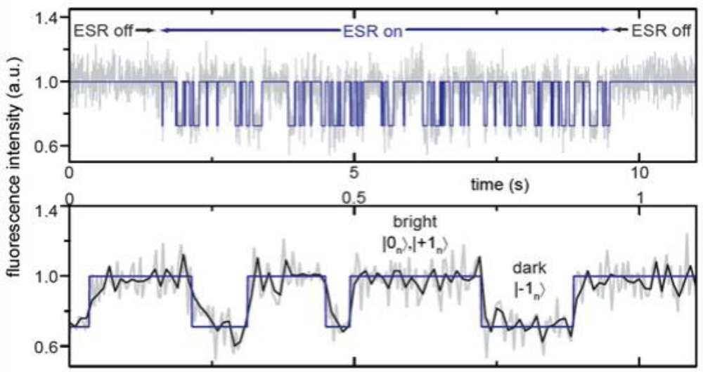
Being able to read out the state of a quantum mechanical object without subsequent destruction of that state is at the heart of numerous quantum feed forward protocols like error correction, entanglement purification. In general a dedicated setting of the measurement device is needed in order to couple strong enough for the readout process to yield a sufficient signal for state identification and yet to preserve the state measured. For the nitrogen-vacancy spin defect in diamond such a setting is achieved for the nitrogen nucleus with an appropriately chosen magnetic field strength and orientation (see Neumann et al. Science 329 (2010) 542ff.). Single shot and quantum non demolition readout of electron spins in this system has not been conclusively demonstrated owing to fast repolarization of the electron spin due to laser excitation and fluorescence readout of the center. However the nitrogen nuclear spin with its hyperfine coupling tensor aligned with the symmetry axis of the electron spin wavefunction is sufficiently decoupled from the electron spin dynamics provided a magnetic field of sufficient strength and orientation along the C 3v center axis is chosen. The work presents a major step towards application of diamond spin defects in quantum science. It might facilitate scaling of spin arrays in the system and even lead to more sensitive parameter estimation in electric and magnetic field measurements.
Original publication:
Title: Single-Shot Readout of a Single Nuclear Spin
Author(s): Neumann,P.,Beck, J., Steiner, M., Rempp, F., Fedder, H., Hemmer, P.R., Wrachtrup, J., Jelezko, F.
Source: Science
Volume: 329
Issue: 5991
Pages: 542 – 544
Published: 30 July 2010
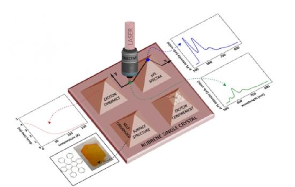
In organic single crystals – in contrast to inorganic systems – the crystal lattice is not stabilized by valence bonds but rather by van-der-Waals forces between the molecules. This yields to optical properties which are fundamentally different from those of inorganic crystalline semiconductors.
Essential questions arising from the properties of weakly bond molecular crystals are the nature of their optical excitations and their spatial transport. In cooperation with scientists from Würzburg, Garching and Cambridge we tackle those questions by studying the photoluminescence (PL) spectra of self-organized surface structures on rubrene single crystals. As a result it appears that the excitonic excitation has to be divided into free i.e. non-localized and so called molecular, “self-trapped” excitons. Spatially resolved intensity measurements along the sides and on the apex of the pyramidal surface structures show an increase of the PL intensity by about one order of magnitude. Beside this strong field enhancement, it is noteworthy that the shape of the PL spectra, and therefore the ratio between free and molecular excitons, changes significantly. This can be explained by spatial confinement of the diffusive transport of free excitons due to scattering at the structure boundaries. By means of temperature-dependent and time-resolved measurements we were able to extract diffusion parameters for free excitons as well as their activation energies for the transition to molecular excitons.
Future studies are to explore the growth mechanism which is behind the forming of this self-organized surface modification.
Original publication:
“Enhanced photoluminescence from self-organized rubrene single crystal surface structures”
by R. J. Stöhr, G. J. Beirne, P. Michler, R. Scholz, J. Wrachtrup, and J. Pflaum
Appl. Phys. Lett. 96, 231902 (2010); doi:10.1063/1.3449124
Die optische Detektion fluoreszenzmarkierter Proteine ermöglicht die Erforschung verschiedenster Prozesse in lebenden Zellen. Eine entscheidende Erweiterung ist die Fluoreszenzanalyse mittels Einzel-Molekül-Techniken wie z.B. die Fluoreszenz-Korrelations-Spektroskopie (FCS). Mit Hilfe von FCS haben wir die topologische Trennung der zwei membranständigen Rezeptorproteine TNFR1 und TNFR2 der Tumor-Necrosis-Factor (TNF) Familie nachweisen können. TNFR1 weist eine langsame Diffusionszeit von 1.2×10⁻⁹ cm2/s, welche sich durch Ligandenstimulierung mit TNF nicht verändert. Überraschenderweise erhöht sich die Diffusion signifikant sobald den Zellen Cholesterol entzogen wurde. Dies deutet auf eine Lokalisierung der TNFR1-Rezeptoren in Cholesterol-reichen Mikrodomänen hin. Im Gegensatz dazu ist die Diffusion von TNFR2 vergleichsweise schnell (D = 3.1×10⁻⁹ cm2/s). Desweiteren ist TNFR2 gekennzeichnet durch eine charakteristische Reduktion der Rezeptordiffusion nach Stimulierung mit TNF (D = 0.9×10⁻⁹ cm2/s). Fluoreszenzintensitätsanalysen haben gezeigt, dass diese Verlangsamung nicht durch die Formation von TNFR2 Clustern erklärt werden kann und dass selbst nach Stimulierung nur wenige Rezeptor Moleküle im Signalkomplex gebunden sind. Unsere Daten weisen deutlich auf eine räumliche Trennung der TNF Rezeptoren in verschiedenen Membrandomänen hin welche unabhängig von der zytoplasmatischen Signaldomäne sind.